LTC1326 View Datasheet(PDF) - Linear Technology
Part Name
Description
Manufacturer
LTC1326 Datasheet PDF : 16 Pages
| |||
LTC1326/LTC1326-2.5
APPLICATIO S I FOR ATIO
During a supply induced reset condition, the ability of the
PBR pin to force a soft reset condition on the SRST pin
is disabled. In other words SRST will remain high. If the
PBR pin is held low, both during and after a supply
induced reset (low RST), the RST pin will remain low until
200ms after the PBR goes high.
Power Detect/Gate Drive
The LTC1326/LTC1326-2.5 for the most part are powered
internally from the VCC3 pin. The exception is at the gate
drive of the output FET on the RST pin. On the input to this
FET is power detection circuitry used to detect and drive
the gate from either the 3.3V input pin (VCC3) or the 5V
input pin (VCC5) on the LTC1326 or the 2.5V input pin
(VCC25) on the LTC1326-2.5. The gate drive is derived
from the pin with the highest potential. This ensures the
part pulls the RST pin low as soon as either input pin is
≥ 1V.
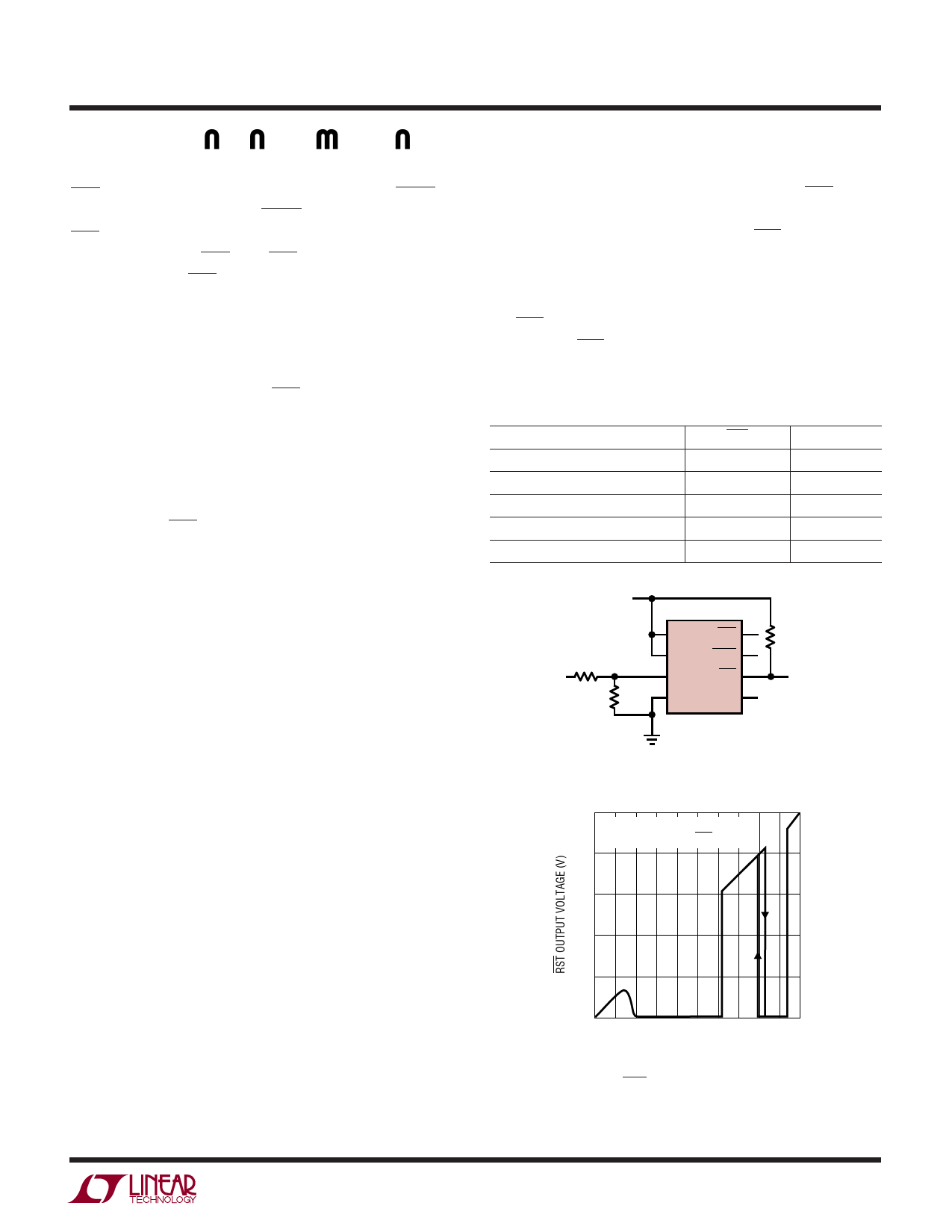
appropriate range. The LTC1326 handles this situation as
shown in Figure 2. Above 1V and below VRT3, RST is held
low. From VRT3 to approximately 4.15V, the LTC1326
assumes 3.3V supply monitoring and RST is deasserted.
Above approximately 4.15V, the LTC1326 operates as a 5V
monitor. In most systems, the 5V supply will pass through
the 3.1V to 4.15V region in <200ms during power-up, and
the RST output will behave as desired. Table 1 summarizes
the state of RST and RST at various operating voltages
with VCC3 = VCC5.
Table 1. Override Truth Table (VCC3 = VCC5)
INPUTS (VCC3 = VCC5 = VCC)
RST
RST
0V ≤ VCC ≤ 1V
—
—
1V ≤ VCC ≤ VRT3
0
1
VRT3 ≤ VCC ≤ 4.15V
1
0
4.15V ≤ VCC ≤ VRT5
0
1
VRT5 ≤ VCC
1
0
Dual and Single Supply Monitor Operation
The VCC3, VCC5 and VCCA inputs may be individually
disabled by the following override techniques which allow
the LTC1326 or LTC1326-2.5 to be used as a dual or single
supply monitor.
LTC1326 Override Functions
The VCCA pin, if unused, can be tied to either VCC3 or VCC5.
This is an obvious solution since the trip points for VCC3
and VCC5 will always be greater than the trip point for VCCA.
The VCC5 input trip point is disabled if its voltage is equal
to the voltage on VCC3 ±25mV and the voltage on VCC5 is
less than 4.15V. In this manner, the part will behave as a
3.3V monitor and the VCC5 reset will be disabled.
The VCC5 trip point is reenabled when the voltage on VCC5
is equal to the voltage on VCC3 ±25mV and the two inputs
are greater than approximately 4.15V. In this manner, the
LTC1326 can function as a 5V monitor with the 3.3V
monitor disabled.
When monitoring either 3.3V or 5V with VCC3 strapped to
VCC5 (see Figure 1), the LTC1326 determines which is the
3.3V OR
5V
ADJUSTABLE R1
SUPPLY
R2
LTC1326
1
VCC3
2
VCC5
3
VCCA
4
GND
8
PBR
7
SRST
6
RST
5
RST
4.7k
SYSTEM RESET
Figure 1
1326/2.5 F01
5
VCC3 = VCC5 = VCCA = 0V TO 5V
4.7k PULL-UP FROM RST TO VCC3
4
3
2
1
0
0
1
2
3
4
5
SUPPLY VOLTAGE (V)
1326/2.5 F02
Figure 2. RST Voltage vs Supply Voltage
132625fc
9
Share Link: 