DSP56852PB View Datasheet(PDF) - Motorola => Freescale
Part Name
Description
Manufacturer
DSP56852PB Datasheet PDF : 44 Pages
| |||
Freescale Semiconductor, Inc.
Introduction
Part 2 Signal/Connection Descriptions
2.1 Introduction
The input and output signals of the DSP56852 are organized into functional groups, as shown in Table 2
and as illustrated in Figure 2. In Table 3 each table row describes the package pin and the signal or signals
present.
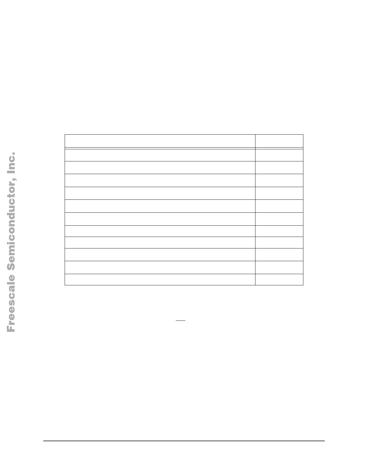
Table 2. Functional Group Pin Allocations
Functional Group
Power (VDD, VDDIO, or VDDA)
Ground (VSS, VSSIO,or VSSA)
Phase Lock Loop (PLL) and Clock
External Bus Signals
External Chip Select*
Interrupt and Program Control
Synchronous Serial Interface (SSI) Port*
Serial Communications Interface (SCI) Port*
Serial Peripheral Interface (SPI) Port
Quad Timer Module Port
JTAG/Enhanced On-Chip Emulation (EOnCE)
*Alternately, GPIO pins
Number of Pins
101
101
22
393
34
35
6
2
06
07
6
1. VDD = VDD CORE, VSS = VSS CORE, VDDIO= VDD IO, VSSIO = VSS IO, VDDA = VDD ANA, VSSA = VSS ANA
2. CLKOUT is muxed Address pin A20.
3. Four Address pins are multiplexed with the timer, CS3 and CLKOUT pins.
4. CS3 is multiplexed with external Address Bus pin A19.
5. Mode pins are multiplexed with External Data pins D13-D15 like A17and A18.
6. Four of these pins are multiplexed with SSI.
7. Two of these pins are multiplexed with 2 bits of the External Address Bus A17and A18.
DSP56852 Technical Data
5
Preliminary
For More Information On This Product,
Go to: www.freescale.com
Share Link: 