DSP56852PB View Datasheet(PDF) - Motorola => Freescale
Part Name
Description
Manufacturer
DSP56852PB Datasheet PDF : 44 Pages
| |||
Freescale Semiconductor, Inc.
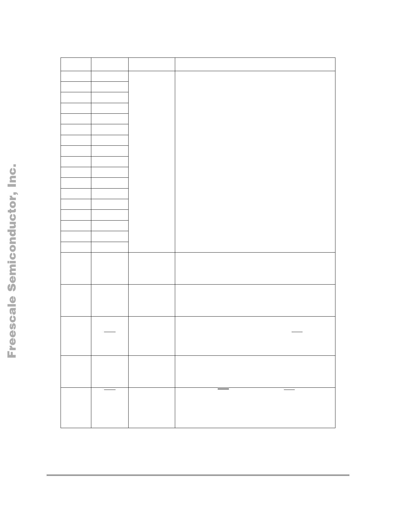
Table 3. DSP56852 Signal and Package Information for the 81-pin MAPBGA
Pin No.
E4
F2
F3
F4
F1
G3
G2
J1
H2
H3
J2
H4
G4
J3
F5
H5
E5
F6
Signal Name
A0
A1
A2
A3
A4
A5
A6
A7
A8
A9
A10
A11
A12
A13
A14
A15
A16
A17
Type
Output(Z)
Output(Z)
Description
Address Bus (A0–A16)—These pins specify a word
address for external program or data memory addresses.
Address Bus (A17)
TIO0
Input/Output Timer I/O (0)—Can be programmed as either a timer input
source or as a timer output flag.
G5
A18
Output(Z) Address Bus (A18)
TIO1
Input/Output Timer I/O (1)—Can be programmed as either a timer input
source or as a timer output flag.
H6
A19
Output(Z) Address Bus (A19)
CS3
J8
CLKO
A20
D2
CS0
Output
Output
Output
Output
External Chip Select 3 —When enabled, a CSx signal is
asserted for external memory accesses that fall within a
programmable address range.
Output clock (CLKO)—User programmable clock out
reference
Address Bus—A20
Chip Select 0 (CS0) —When enabled, a CSx signal is
asserted for external memory accesses that fall within a
programmable address range.
GPIOA0
Input/Output Port A GPIO (0) —A general purpose IO pin.
8
DSP56852 Technical Data
For More Information On This Product,
Preliminary
Go to: www.freescale.com
Share Link: 