DSP56852PB View Datasheet(PDF) - Motorola => Freescale
Part Name
Description
Manufacturer
DSP56852PB Datasheet PDF : 44 Pages
| |||
Freescale Semiconductor, Inc.
Introduction
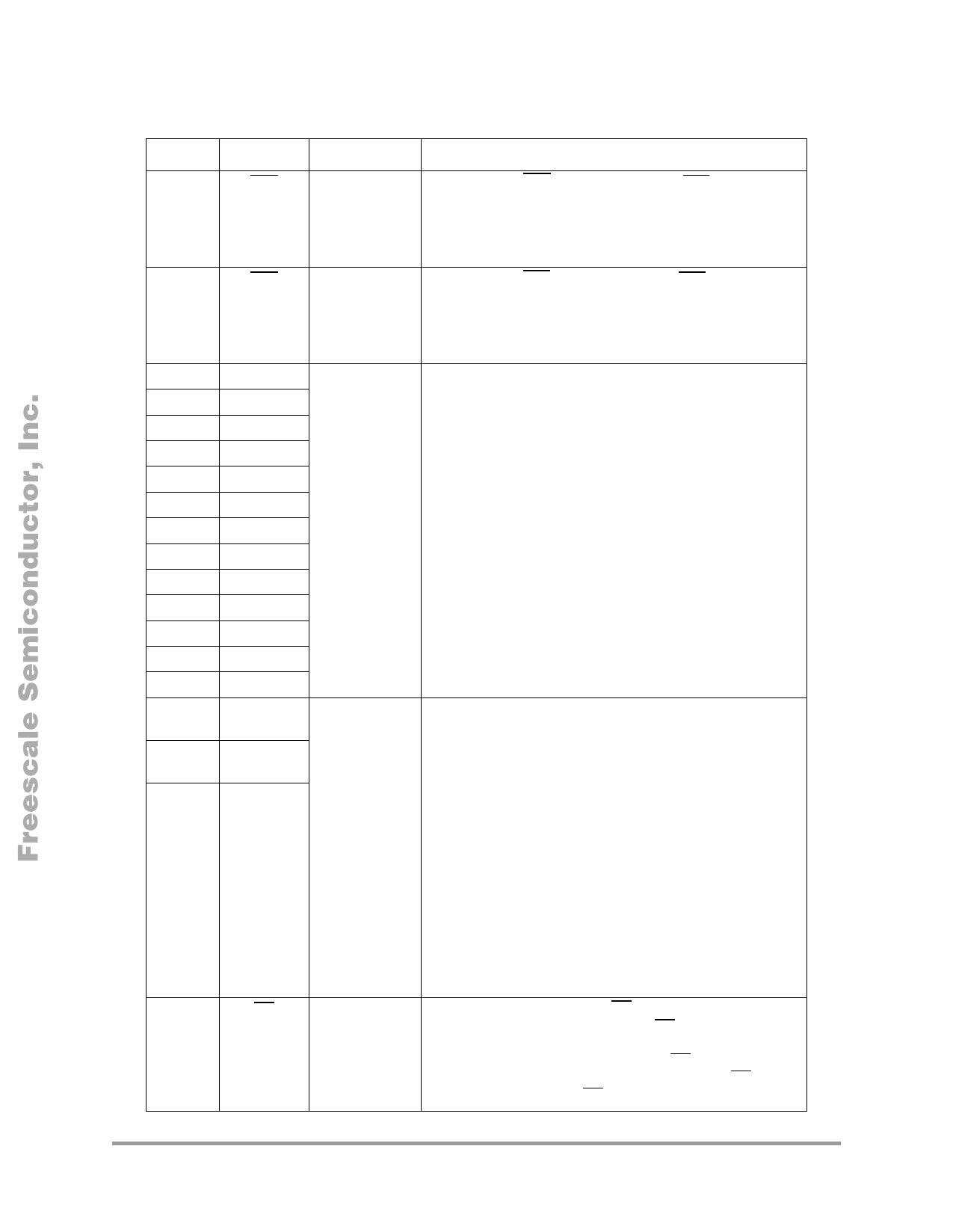
Table 3. DSP56852 Signal and Package Information for the 81-pin MAPBGA
Pin No.
D3
Signal Name
CS1
Type
Output
Description
Chip Select 1 (CS1) —When enabled, a CSx signal is
asserted for external memory accesses that fall within a
programmable address range.
GPIOA1
Input/Output Port A GPIO (1) —A general purpose IO pin.
C3
CS2
Output
Chip Select 2 (CS2)—When enabled, a CSx signal is
asserted for external memory accesses that fall within a
programmable address range.
GPIOA2
Input/Output Port A GPIO (2) —A general purpose IO pin.
G7
D0
Input/Output Data Bus (D0–D12) —specify the data for external program or
H7
D1
data memory accesses. D0–D15 are tri-stated when the
external bus is inactive.
H8
D2
G8
D3
H9
D4
F8
D5
F7
D6
G6
D7
E8
D8
E7
D9
E6
D10
D8
D11
D7
D12
D9
D13
Input/Output Data Bus (D13–D15) — specify the data for external program
MODE A
or data memory accesses. D0–D15 are tri-stated when the
C8
D14
external bus is inactive.
MODE B
Mode Select—During the bootstrap process the MODE A,
A9
D15
MODE B, and MODE C pins select one of the eight
MODE C
bootstrap modes. These pins are sampled at the end of
reset.
Note: Any time POR and EXTERNAL resets are active, the
state of MODE A, B and C pins get asynchronously
transferred to the SIM Control Register [14:12] ($1FFF08)
respectively. These bits determine the mode in which the
part will boot up.
E2
RD
Output
Note: Software and COP resets do not update the SIM
Control Register.
Bus Control– Read Enable (RD)—is asserted during
external memory read cycles. When RD is asserted low,
pins D0–D15 become inputs and an external device is
enabled onto the DSP data bus. When RD is deasserted
high, the external data is latched inside the DSP. RD can be
connected directly to the OE pin of a Static RAM or ROM.
DSP56852 Technical Data
9
Preliminary
For More Information On This Product,
Go to: www.freescale.com
Share Link: 