MCM72BA32SG50 View Datasheet(PDF) - Motorola => Freescale
Part Name
Description
Manufacturer
MCM72BA32SG50 Datasheet PDF : 14 Pages
| |||
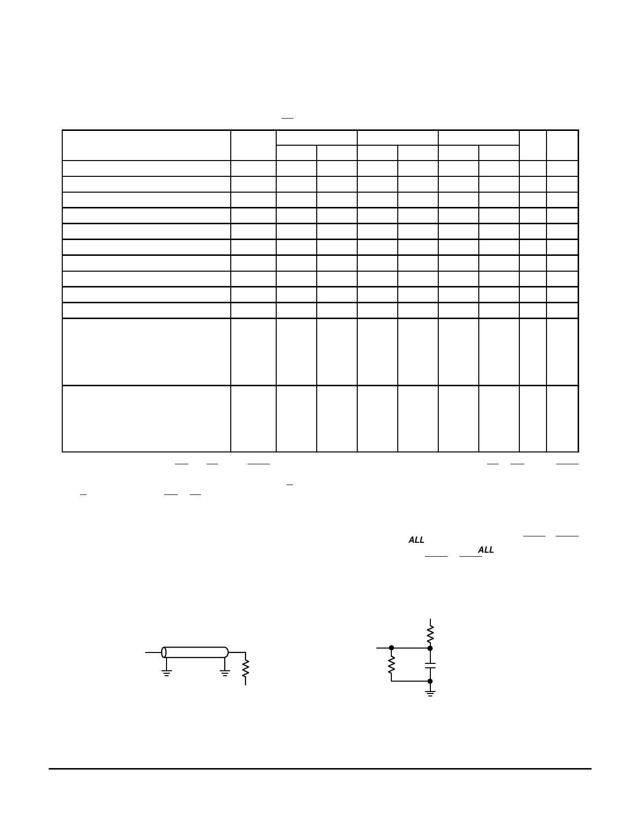
AC OPERATING CONDITIONS AND CHARACTERISTICS
(VCC = 5.0 V ± 5%, TA = 0 to + 70°C, Unless Otherwise Noted)
Input Timing Measurement Reference Level . . . . . . . . . . . . . . . 1.5 V
Input Pulse Levels . . . . . . . . . . . . . . . . . . . . . . . . . . . . . . . . . 0 to 3.0 V
Input Rise/Fall Time . . . . . . . . . . . . . . . . . . . . . . . . . . . . . . . . . . . . 3 ns
Output Timing Reference Level . . . . . . . . . . . . . . . . . . . . . . . . . . 1.5 V
Output Load . . . . . . . . . . . . See Figure 1A Unless Otherwise Noted
READ/WRITE CYCLE TIMING (See Notes 1, 2, and 3) (Wx refers to any or all byte write enables)
MCM72BA64SG66 MCM72BA64SG60 MCM72BA64SG50
Parameter
Symbol Min
Max
Min
Max
Min
Max Unit Notes
Cycle Time
tKHKH
15
—
16.7
—
20
—
ns
Clock Access Time
tKHQV
—
9
—
10
—
12
ns
4
Output Enable to Output Valid
tGLQV
—
5
—
5
—
6
ns
Clock High to Output Active
tKHQX1
6
—
6
—
6
—
ns
Clock High to Output Change
tKHQX2
3
—
3
—
3
—
ns
Output Enable to Output Active
tGLQX
0
—
0
—
0
—
ns
Output Disable to Q High–Z
tGHQZ
2
6
2
6
2
7
ns
5
Clock High to Q High–Z
tKHQZ
—
6
—
6
—
6
ns
Clock High Pulse Width
tKHKL
5
—
5
—
6
—
ns
Clock Low Pulse Width
tKLKH
5
—
5
—
6
—
ns
Setup Times:
Address tAVKH
2.5
—
2.5
—
2.5
—
ns
6
Address Status tADSVKH
Data In tDVKH
Write tWVKH
Address Advance tADVVKH
Chip Enable tEVKH
Hold Times:
Address tKHAX
0.5
—
0.5
—
0.5
—
ns
6
Address Status tKHADSX
Data In tKHDX
Write tKHWX
Address Advance tKHADVX
Chip Enable tKHEX
NOTES:
1. A read cycle is defined by UW and LW high or ADSP low for the setup and hold times. A write cycle is defined by LW or UW low and ADSP
high for the setup and hold times.
2. All read and write cycle timings are referenced from K or G.
3. G is a don’t care when UW or LW is sampled low.
4. Maximum access times are guaranteed for all possible Pentium external bus cycles.
5. Transition is measured ± 500 mV from steady–state voltage with load of Figure 1B. This parameter is sampled rather than 100% tested. At
any given voltage and temperature, tKHQZ max is less than tKHQZ1 min for a given device and from device to device.
6. This is a synchronous device. All addresses must meet the specified setup and hold times for ALL rising edges of K whenever ADSP or ADSC
is low, and the chip is selected. All other synchronous inputs must meet the specified setup and hold times for ALL rising edges of K when
the chip is enabled.Chip enable must be valid at each rising edge of clock for the device (when ADSP or ADSC is low) to remain enabled.
OUTPUT
AC TEST LOADS
Z0 = 50 Ω
RL = 50 Ω
VL = 1.5 V
Figure 1A
OUTPUT
255 Ω
+5V
480 Ω
5 pF
Figure 1B
MCM72BA32•MCM72BA64
8
MOTOROLA FAST SRAM
Share Link: 