MCM64PC32 View Datasheet(PDF) - Motorola => Freescale
Part Name
Description
Manufacturer
MCM64PC32 Datasheet PDF : 16 Pages
| |||
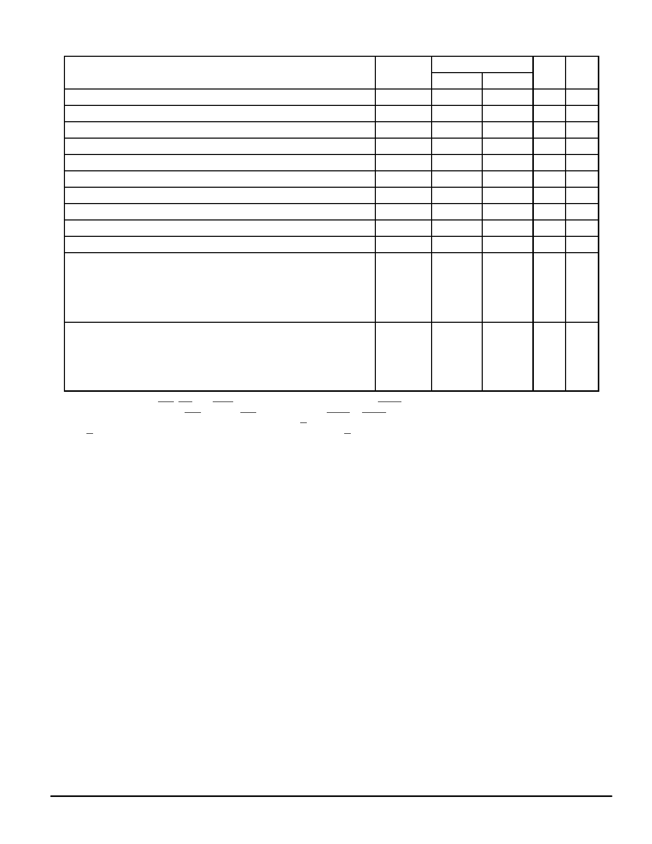
DATA RAMs READ/WRITE CYCLE TIMING (See Notes 1, 2, and 3)
MCM64PC32–66
Parameter
Symbol
Min
Max
Cycle Time
tKHKH
15
—
Clock Access Time
tKHQV
—
8
Output Enable to Output Valid
tGLQV
—
6
Clock High to Output Active
tKHQX1
0
—
Clock High to Output Change
tKHQX2
2
—
Output Enable to Output Active
tGLQX
0
—
Output Disable to Q High–Z
tGHQZ
—
8
Clock High to Q High–Z
tKHQZ
2
8
Clock High Pulse Width
tKHKL
5
—
Clock Low Pulse Width
tKLKH
5
—
Setup Times:
Address tAVKH
2.5
—
Address Status tADSVKH
Data In tDVKH
Write tWVKH
Address Advance tADVVKH
Chip Enable tEVKH
Hold Times:
Address tKHAX
0.5
—
Address Status tKHADSX
Data In tKHDX
Write tKHWX
Address Advance tKHADVX
Chip Enable tKHEX
NOTES:
1. Write applies to all SBx, SW, and SGW signals when the chip is selected and ADSP high.
2. Chip Enable applies to all SE1, SE2 and SE3 signals whenever ADSP or ADSC is asserted.
3. All read and write cycle timings are referenced from K or G.
4. G is a don’t care after write cycle begins. To prevent bus contention, G should be negated prior to start of write cycle.
5. Tested per AC Test Load.
6. Measured at ± 200 mV from steady state. Tested per High–Z Test Load.
7. This parameter is sampled and is not 100% tested.
Unit Notes
ns
ns
5
ns
5
ns 5, 7
ns 5, 7
ns 5, 7
ns 6, 7
ns 6, 7
ns
ns
ns
4
ns
4
MOTOROLA FAST SRAM
MCM64PC32•MCM64PC64
9
Share Link: 