MCM72CF32SG66 View Datasheet(PDF) - Motorola => Freescale
Part Name
Description
Manufacturer
MCM72CF32SG66 Datasheet PDF : 14 Pages
| |||
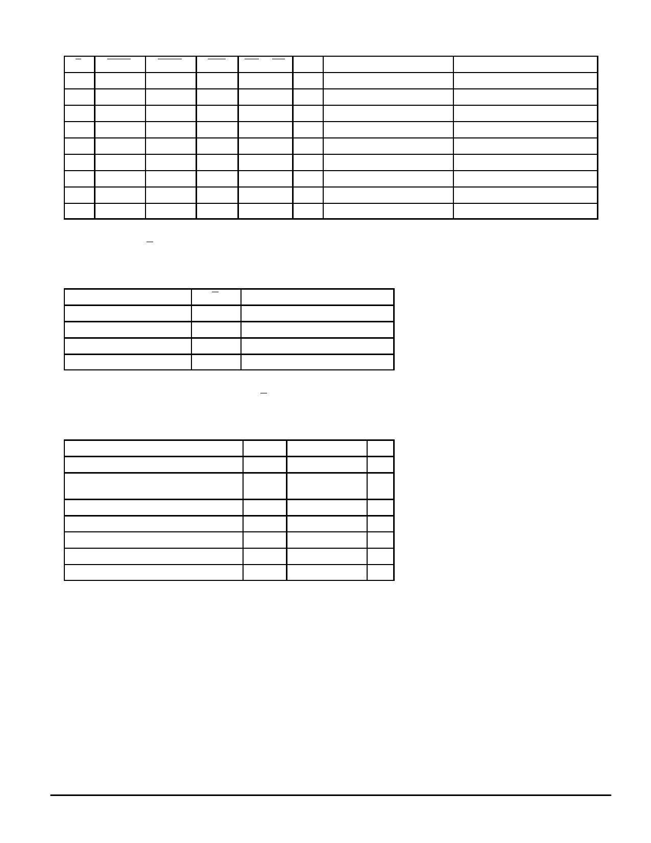
SYNCHRONOUS TRUTH TABLE (See Notes 1, 2, and 3)
E
ADSP
ADSC
ADV UW or LW K
Address Used
H
L
X
X
X
L–H
N/A
H
X
L
X
X
L–H
N/A
L
L
X
X
X
L–H
External Address
L
H
L
X
L
L–H
External Address
L
H
L
X
H
L–H
External Address
X
H
H
L
L
L–H
Next Address
X
H
H
L
H
L–H
Next Address
X
H
H
H
L
L–H
Current Address
X
H
H
H
H
L–H
Current Address
NOTES:
1. X means Don’t Care.
2. All inputs except G must meet setup and hold times for the low–to–high transition of clock (K).
3. Wait states are inserted by suspending burst.
Operation
Deselected
Deselected
Read Cycle, Begin Burst
Write Cycle, Begin Burst
Read Cycle, Begin Burst
Write Cycle, Continue Burst
Read Cycle, Continue Burst
Write Cycle, Suspend Burst
Read Cycle, Suspend Burst
ASYNCHRONOUS TRUTH TABLE (See Notes 1 and 2)
Operation
G
I/O Status
Read
L
Data Out
Read
H
High–Z
Write
X
High–Z — Data In
Deselected
X
High–Z
NOTES:
1. X means Don’t Care.
2. For a write operation following a read operation, G must be high before the input data
required setup time and held high through the input data hold time.
ABSOLUTE MAXIMUM RATINGS (Voltages Referenced to VSS = 0 V)
Rating
Symbol
Value
Unit
Power Supply Voltage
Voltage Relative to VSS for Any
Pin Except VCC
VCC
– 0.5 to + 7.0
V
Vin, Vout – 0.5 to VCC + 0.5 V
Output Current (per I/O)
Iout
± 30
mA
Power Dissipation
PD
6.4
W
Temperature Under Bias
Tbias
– 10 to + 85
°C
Operating Temperature
TA
0 to +70
°C
Storage Temperature
Tstg
– 55 to + 125
°C
NOTE: Permanent device damage may occur if ABSOLUTE MAXIMUM RATINGS are
exceeded. Functional operation should be restricted to RECOMMENDED OPER-
ATING CONDITIONS. Exposure to higher than recommended voltages for
extended periods of time could affect device reliability.
This device contains circuitry to protect the
inputs against damage due to high static volt-
ages or electric fields; however, it is advised
that normal precautions be taken to avoid
application of any voltage higher than maxi-
mum rated voltages to this high–impedance
circuit.
This device contains circuitry that will ensure
the output devices are in High–Z at power up.
MCM72CF32•MCM72CF64
6
MOTOROLA FAST SRAM
Share Link: 