APU4003 View Datasheet(PDF) - APLUS INTEGRATED CIRCUITS
Part Name
Description
Manufacturer
APU4003 Datasheet PDF : 9 Pages
| |||
APU4003
Pin Description
Pin Name
OSCIN
OSCOUT
CAP
S1~4
M1~4
P1~4
IOA1~4
IOB1~4
INT
RESET
LIGHT
ALARM
VDD
GND
VSS0
VSS1
VSS2
VSS3
CUP1~2
COM1~3
SEG1~25
TESTA
Type
I
O
I
I
I
O
I/O
I/O
I
I
O
O
O
O
O
*
Description
Typical 32.768kHz crystal is connected across OSCIN/OSCOUT for Oscillation; R/C
oscillation mode also available.
Connected to OSCOUT for compensation capacitor.
Port for input only with chattering eliminator for CK10 (32ms), CK8 (8ms) & CK6
(2ms). (PLA mask option).
Input ports.
Output ports.
Input/Output ports. After power-on reset, sets as input mode.
Input/Output ports. After power-on reset, sets as input mode.
External interrupt request control input pin.
System reset pin.
Output only for outputting signal to drive transistor for light.
Output only for outputting 4kHz/2kHz/1kHz modulation signal. Also can be used to
output a non-modulation signal.
(+)Power supply pin.
Power supply pin for logic unit inside LSI. When using Li version, a capacitor must be
connected across GND and VDD to prevent the logic unit from malfunctioning.
(--) Power supply pin.
* For Ag version, apply (--) side to both VSS0 & VSS1.
For other than Ag version, apply (--) side to both VSS0 & VSS2.
LCD power supply pin.
Pins for connecting the voltage step-up (step-down) capacitor.
Output pins for LCD panel common plate.
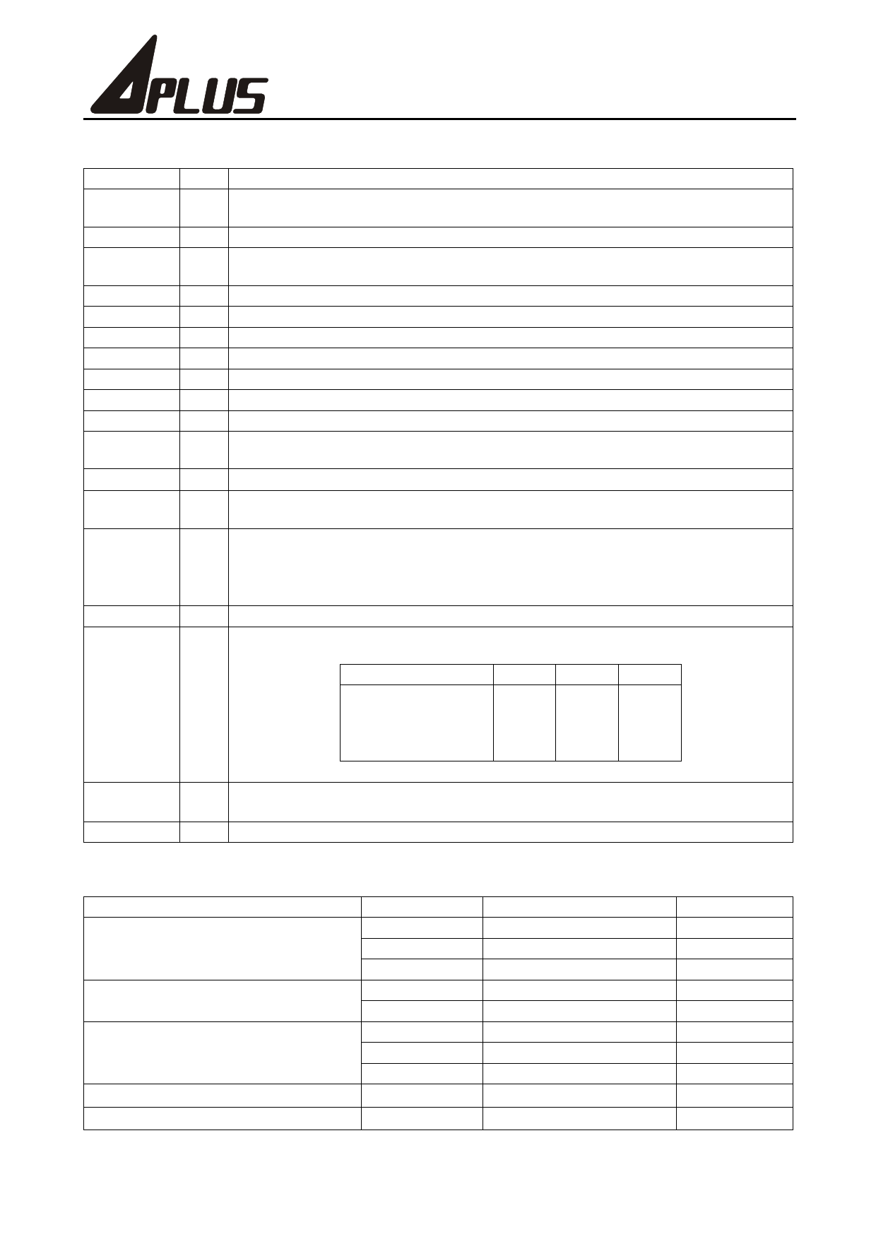
The following pin is used in each case.
Statuc 1/2 duty 1/3 duty
COM1
0
COM2
Ё
COM3
Ё
Alternating Frequency 32Hz*
0
0
Ё
32Hz*
0
0
0
43Hz*
* Frequency can be doubled, quadrupled with PLA.
Output pins for LCD panel segments.
* Also used as output ports with mask option.
Test pin (for internal testing only).
Absolute Maximum Rating
Name
Maximum Supply Voltage
Maximum Input Voltage
Maximum Output Voltage
Maximum Operating Temperature
Maximum Storage Temperature
Preliminary
Symbol
VSS1
VSS2
VSS3
VIN1
VIN2
VOUT1
VOUT2
VOUT3
tOPG
tSTG
3
Ta = 0 to 70к, VDD=0V
Rating
-5.5 ~ +0.3
-5.5 ~ +0.3
-8.5 ~ +0.3
VSS1-0.3 to +0.3
VSS2-0.3 to +0.3
VSS1-0.3 to +0.3
VSS2-0.3 to +0.3
VSS3-0.3 to +0.3
0 to +70
-25 to +125
Unit
V
V
V
V
V
V
V
V
к
к
Ver. 0.0
Share Link: 