IDT79R4650(1996) View Datasheet(PDF) - Integrated Device Technology
Part Name
Description
Manufacturer
IDT79R4650 Datasheet PDF : 22 Pages
| |||
IDT79R4650
enters kernel mode at reset, and whenever an exception is
recognized.
User mode is typically used for applications programs.
User mode accesses are limited to a subset of the virtual
address space, and can be inhibited from accessing CP0
functions.
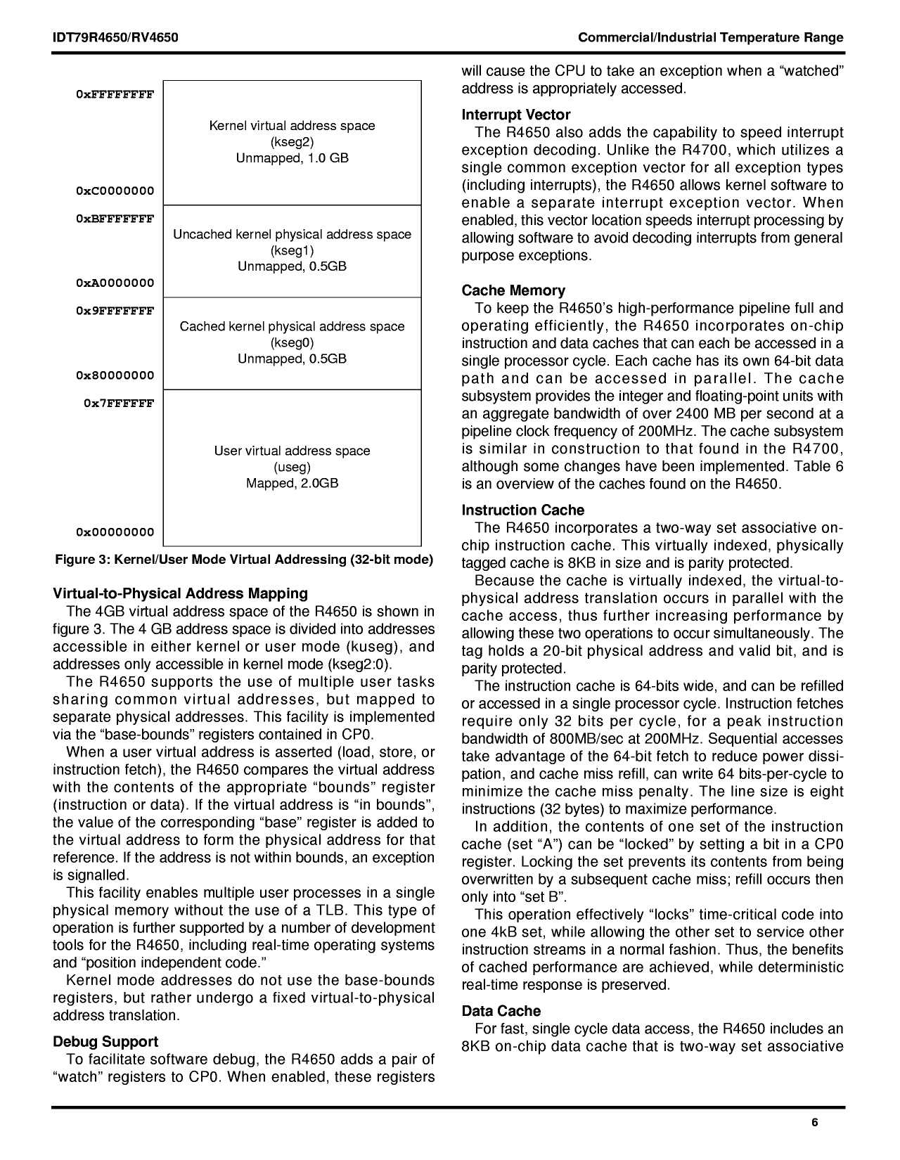
0xFFFFFFFF
Kernel virtual address space
(kseg2)
Unmapped, 1.0 GB
0xC0000000
0xBFFFFFFF
0xA0000000
Uncached kernel physical address space
(kseg1)
Unmapped, 0.5GB
0x9FFFFFFF
0x80000000
Cached kernel physical address space
(kseg0)
Unmapped, 0.5GB
0x7FFFFFF
User virtual address space
(useg)
Mapped, 2.0GB
0x00000000
Figure 3: Mode Virtual Addressing (32-bit mode)
Virtual to Physical Address Mapping
The 4GB virtual address space of the R4650 is shown in
figure 3. The 4 GB address space is divided into addresses
accessible in either kernel or user mode (kuseg), and
addresses only accessible in kernel mode (kseg2:0).
The R4650 supports the use of multiple user tasks
sharing common virtual addresses, but mapped to
separate physical addresses. This facility is implemented
via the “base-bounds” registers contained in CP0.
When a user virtual address is asserted (load, store, or
instruction fetch), the R4650 compares the virtual address
with the contents of the appropriate “bounds” register
(instruction or data). If the virtual address is “in bounds”,
the value of the corresponding “base” register is added to
the virtual address to form the physical address for that
reference. If the address is not within bounds, an exception
is signalled.
This facility enables multiple user processes in a single
physical memory without the use of a TLB. This type of
operation is further supported by a number of development
tools for the R4650, including real-time operating systems
and “position independent code”.
COMMERCIAL TEMPERATURE RANGE
Kernel mode addresses do not use the base-bounds
registers, but rather undergo a fixed virtual to physical
address translation.
Debug Support
To facilitate software debug, the R4650 adds a pair of
“watch” registers to CP0. When enabled, these registers
will cause the CPU to take an exception when a “watched”
address is appropriately accessed.
Interrupt Vector
The R4650 also adds the capability to speed interrupt
exception decoding. Unlike the R4600, which utilizes a
single common exception vector for all exception types
(including interrupts), the R4650 allows kernel software to
enable a separate interrupt exception vector. When
enabled, this vector location speeds interrupt processing by
allowing software to avoid decoding interrupts from general
purpose exceptions.
Cache Memory
In order to keep the R4650’s high-performance pipeline
full and operating efficiently, the R4650 incorporates on-
chip instruction and data caches that can each be
accessed in a single processor cycle. Each cache has its
own 64-bit data path and can be accessed in parallel. The
cache subsystem provides the integer and floating-point
units with an aggregate bandwidth of over 1500 MB per
second at a pipeline clock frequency of 133MHz. The
cache subsystem is similar in construction to that found in
the R4600, although some changes have been imple-
mented. Table 6 is an overview of the caches found on the
R4650.
Instruction Cache
The R4650 incorporates a two-way set associative on-
chip instruction cache. This virtually indexed, physically
tagged cache is 8KB in size and is parity protected.
Because the cache is virtually indexed, the virtual-to-
physical address translation occurs in parallel with the
cache access, thus further increasing performance by
allowing these two operations to occur simultaneously. The
tag holds a 20-bit physical address and valid bit, and is
parity protected.
The instruction cache is 64-bits wide, and can be refilled
or accessed in a single processor cycle. Instruction fetches
require only 32 bits per cycle, for a peak instruction
bandwidth of 533MB/sec at 133MHz. Sequential accesses
take advantage of the 64-bit fetch to reduce power dissi-
pation, and cache miss refill, can write 64 bits-per-cycle to
minimize the cache miss penalty. The line size is eight
instructions (32 bytes) to maximize performance.
In addition, the contents of one set of the instruction
cache (set “A”) can be “locked” by setting a bit in a CP0
register. Locking the set prevents its contents from being
overwritten by a subsequent cache miss; refill occurs then
only into “set B”.
This operation effectively “locks” time critical code into
one 4kB set, while allowing the other set to service other
instruction streams in a normal fashion. Thus, the benefits
5.8
6
Share Link: 