IDT79R4650-180DP View Datasheet(PDF) - Integrated Device Technology
Part Name
Description
Manufacturer
IDT79R4650-180DP Datasheet PDF : 25 Pages
| |||
IDT79RC4650™
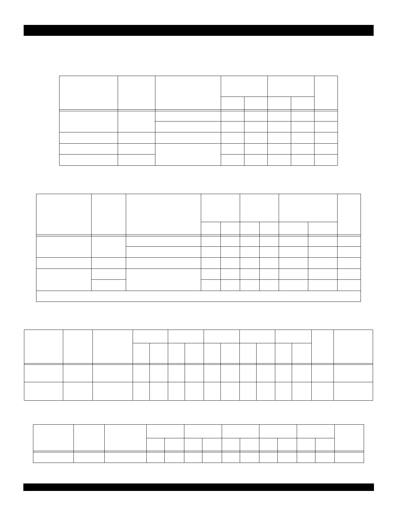
System Interface Parameters—RV4650
(VCC=3.3V ± 5%; Commercial TCASE = 0°C to +85°C, Industrial TCASE = -40°C to +85°C)
Note: Timings are measured from 1.5V of the clock to 1.5V of the signal.
Parameter
Symbol
Test Conditions
Data Output1
Data Output Hold
tDM= Min
tDO = Max
tDOH2
mode14..13 = 10 (fastest)
mode14..13 = 01 (slowest)
mode14..13 = 10 (fastest)
Input Data Setup
tDS
Input Data Hold
tDH
trise = 5ns
tfall = 5ns
1. Capacitive load for all output timings is 50pF.
2. 50pf loading on external output signals, fastest settings
RV4650
133/67MHz
Min
0
0
0
4.5
1.5
Max
9
12
—
—
—
RV4650
150/75MHz
Min
0
0
0
4.5
1.5
Max
9
12
—
—
—
Units
ns
ns
ns
ns
ns
Parameter
Symbol
Test Conditions
Data Output
tDM= Min
tDO = Max
mode14..13 = 10 (fastest)
mode14..13 = 01 (slowest)
Data Output Hold
tDOH*
mode14..13 = 10 (fastest)
Data Input
tDS
trise = 3ns
tDH
tfall = 3ns
50pf loading on external output signals, fastest settings
RV4650
180/
90MHz
RV4650
200/
100MHz
RV4650
267/89MHz
Min Max Min Max Min
0
9
0
4.5 0
0
10 0
5.0 0
0
—
0
—
0
4.5 —
4.5 —
2.5
1.5 —
1.5 —
1.0
Max
4.5
5.0
—
—
—
Units
ns
ns
ns
ns
ns
Boot Time Interface Parameters—RV4650
Parameter
Symbol
Test
Conditions
133MHz
Min
Ma
x
150MHz 180MHz 200MHz 267MHz
Units Conditions
Min Max Min Max Min Max Min Max
Mode Data
tDS
—
Setup
3
—3
—
3
—
3
—
3
—
ns
Master Clock
Cycle
Mode Data
tDH
—
Hold
0
—0
—
0
—
0
—
0
—
ns
Master Clock
Cycle
Capacitive Load Deration—RV4650
Parameter
Symbol
Test
Conditions
133MHz 150MHz 180MHz 200MHz 267MHz
Min Max Min Max Min Max Min Max Min Max
Units
Load Derate
CLD
—
—2
—2
—2
—2
—1
ns/25pF
18 of 25
April 10, 2001
Share Link: 