IDT79R4650-180DP View Datasheet(PDF) - Integrated Device Technology
Part Name
Description
Manufacturer
IDT79R4650-180DP Datasheet PDF : 25 Pages
| |||
IDT79RC4650™
Instruction Cache
The RC4650 incorporates a two-way set associative on-chip instruc-
tion cache. This virtually indexed, physically tagged cache is 8KB in size
and is parity protected.
Because the cache is virtually indexed, the virtual-to-physical
address translation occurs in parallel with the cache access, thus further
increasing performance by allowing these two operations to occur simul-
taneously. The tag holds a 20-bit physical address and valid bit, and is
parity protected.
The instruction cache is 64-bits wide, and can be refilled or accessed
in a single processor cycle. Instruction fetches require only 32 bits per
cycle, for a peak instruction bandwidth of 1068MB/sec at 267MHz.
Sequential accesses take advantage of the 64-bit fetch to reduce power
dissipation, and cache miss refill, can write 64 bits-per-cycle to minimize
the cache miss penalty. The line size is eight instructions (32 bytes) to
maximize performance.
In addition, the contents of one set of the instruction cache (set “A”)
can be “locked” by setting a bit in a CP0 register. Locking the set
prevents its contents from being overwritten by a subsequent cache
miss; refill occurs then only into “set B”.
This operation effectively “locks” time-critical code into one 4kB set,
while allowing the other set to service other instruction streams in a
normal fashion. Thus, the benefits of cached performance are achieved,
while deterministic real-time response is preserved.
Data Cache
For fast, single cycle data access, the RC4650 includes an 8KB on-
chip data cache that is two-way set associative with a fixed 32-byte
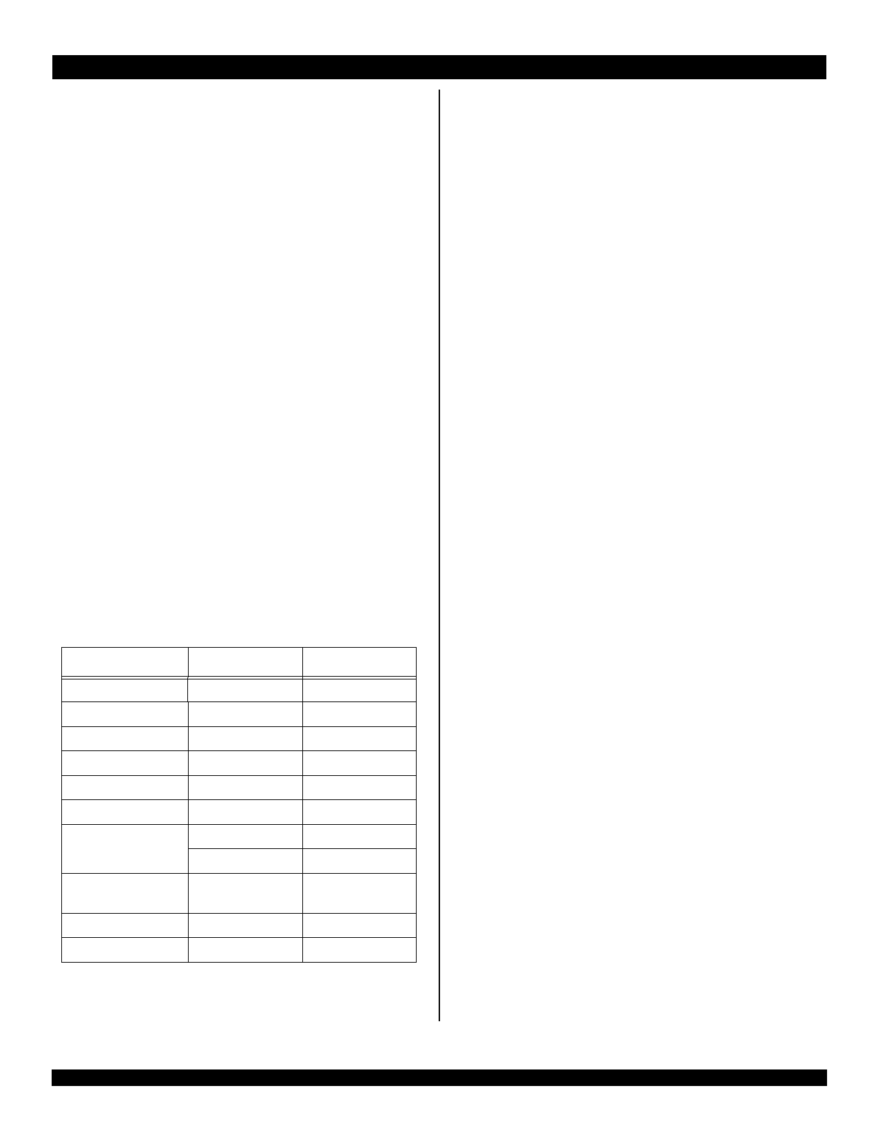
(eight words) line size. Table 4 lists the RC4650 cache attributes.
Characteristics Instruction
Data
Size
Organization
Line size
Index
Tag
Write policy
Line transfer order
Miss restart after
transfer of
Parity
Cache locking
8KB
8KB
2-way set associative 2-way set associative
32B
32B
vAddr11..0
pAddr31..12
n.a.
vAddr11..0
pAddr31..12
writeback /writethru
read sub-block order read sub-block order
write sequential
write sequential
entire line
first word
per-word
set A
per-byte
set A
Table 4 RC4650 Cache Attributes
The data cache is protected with byte parity and its tag is protected
with a single parity bit. It is virtually indexed and physically tagged to
allow simultaneous address translation and data cache access
The normal write policy is writeback, which means that a store to a
cache line does not immediately cause memory to be updated. This
increases system performance by reducing bus traffic and eliminating
the bottleneck of waiting for each store operation to finish before issuing
a subsequent memory operation. Software can however select write-
through for certain address ranges, using the CAlg register in CP0.
Cache protocols supported for the data cache are:
Uncached. Addresses in a memory area indicated as uncached will
not be read from the cache. Stores to such addresses will be written
directly to main memory, without changing cache contents.
x Writeback. Loads and instruction fetches will first search the
cache, reading main memory only if the desired data is not
cache resident. On data store operations, the cache is first
searched to see if the target address is cache resident. If it is
resident, the cache contents will be updated, and the cache line
marked for later writeback. If the cache lookup misses, the
target line is first brought into the cache before the cache is
updated.
x Write-through with write allocate. Loads and instruction
fetches will first search the cache, reading main memory only if
the desired data is not cache resident. On data store operations,
the cache is first searched to see if the target address is cache
resident. If it is resident, the cache contents will be updated and
main memory will also be written; the state of the “writeback” bit
of the cache line will be unchanged. If the cache lookup misses,
the target line is first brought into the cache before the cache is
updated.
x Write-through without write-allocate. Loads and instruction
fetches will first search the cache, reading main memory only if
the desired data is not cache resident. On data store operations,
the cache is first searched to see if the target address is cache
resident. If it is resident, the cache contents will be updated, and
the cache line marked for later writeback. If the cache lookup
misses, then only main memory is written.
Associated with the Data Cache is the store buffer. When the
RC4650 executes a Store instruction, this single-entry buffer gets
written with the store data while the tag comparison is performed. If the
tag matches, then the data is written into the Data Cache in the next
cycle that the Data Cache is not accessed (the next non-load cycle).
The store buffer allows the RC4650 to execute a store every processor
cycle and to perform back-to-back stores without penalty.
Write Buffer
Writes to external memory, whether cache miss writebacks or stores
to uncached or write-through addresses, use the on-chip write buffer.
The write buffer holds up to four address and data pairs. The entire
buffer is used for a data cache writeback and allows the processor to
proceed in parallel with memory update.
6 of 25
April 10, 2001
Share Link: 