TXM-418-LC View Datasheet(PDF) - Unspecified
Part Name
Description
Manufacturer
TXM-418-LC Datasheet PDF : 11 Pages
| |||
ELECTRICAL SPECIFICATIONS
Parameter
POWER SUPPLY
Operating Voltage
Supply Current
Power-down Current
TRANSMITTER SECTION
Transmit Frequency:
TXM-315-LC
TXM-418-LC
TXM-433-LC
Center Frequency Accuracy
Output Power
Harmonic Emissions
Data Rate
Data Input:
Logic Low
Logic High
ANTENNA PORT
RF Output Impedance
TIMING
Transmitter Turn-On Time
Transmitter Turn-Off Time
ENVIRONMENTAL
Operating Temperature Range
Designation Min.
VCC
2.7
ICC
–
IPDN
–
FC
–
–
–
–
-50
Po
-4
PH
–
–
100
VIL
0.0
VIH
2.5
ROUT
–
–
–
–
–
–
-30
Table 1: LC Series Transmitter Specifications
Notes
1. Current draw with DATA pin held continuously high.
2. Current draw with DATA pin low.
3. RF out connected to a 50Ω load.
4. LADJ through 430Ω resistor.
5. Characterized, but not tested.
Typical
Max.
–
5.2
3.0
6.0
–
1.5
315
418
433.92
–
0
–
–
–
–
50
30
–
–
–
–
–
+50
+4
-40
5,000
0.4
Vcc
–
80
100
+70
Units Notes
VDC
–
mA
1,4
µA
2
MHz
–
MHz
–
MHz
–
kHz
–
dBm
3
dBc
3
bps
–
VDC
–
VDC
–
Ω
5
µSec
5
nSec
5
°C
5
ABSOLUTE MAXIMUM RATINGS
Supply Voltage VCC
Any Input or Output Pin
Operating Temperature
Storage Temperature
Soldering Temperature
-0.3
to +6.0
-0.3
to
VCC
-30
to
+70
-45
to
+85
+225°C for 10 seconds
VDC
VDC
°C
°C
*NOTE* Exceeding any of the limits of this section may lead to permanent
damage to the device. Furthermore, extended operation at these maximum
ratings may reduce the life of this device.
Page 2
*CAUTION*
This product incorporates numerous static-sensitive components.
Always wear an ESD wrist strap and observe proper ESD handling
procedures when working with this device. Failure to observe this
precaution may result in module damage or failure.
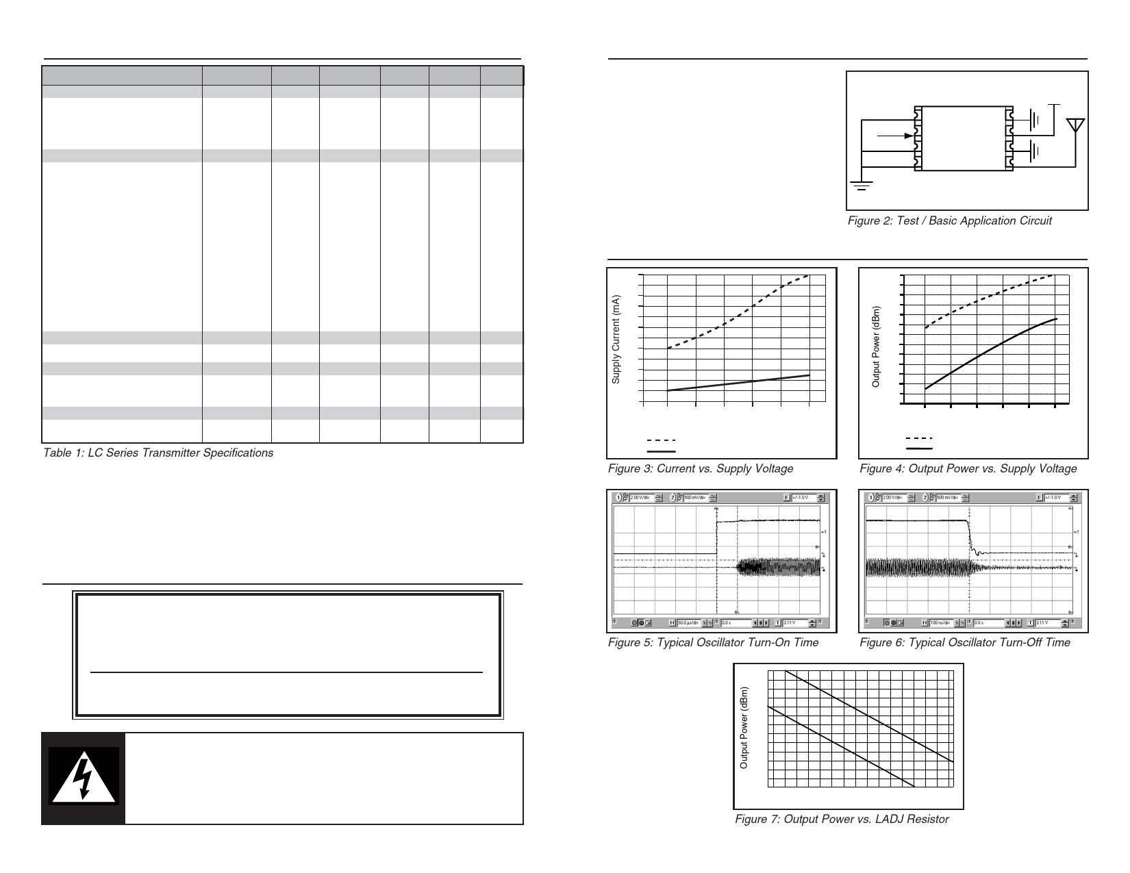
PERFORMANCE DATA
These performance parameters
are based on module operation at
25°C from a 3.3VDC supply unless
otherwise noted. Figure 2
illustrates the connections
necessary for testing and
operation. It is recommended all
ground pins be connected to the
ground plane.
VCC
1 GND
GND 8
2 DATA VCC 7
3 GND
GND 6
4 LADJ/GND ANT 5
Figure 2: Test / Basic Application Circuit
TYPICAL PERFORMANCE GRAPHS
12
11
10
9
8
7
6
5
4
3
2
1
0
2.5 3.0 3.5 4.0 4.5 5.0
Supply Voltage (V)
With LADJ tied to ground
With 430Ω resistor on LADJ
Figure 3: Current vs. Supply Voltage
+8
+7
+6
+5
+4
+3
+2
+1
0
-1
-2
-3
-4
-5
2.5 3.0 3.5 4.0 4.5 5.0
Supply Voltage (V)
With LADJ tied to ground
With 430Ω resistor on LADJ
Figure 4: Output Power vs. Supply Voltage
Data
Carrier
Data
Carrier
Figure 5: Typical Oscillator Turn-On Time
Figure 6: Typical Oscillator Turn-Off Time
+8
+7
+6
+5
+4
+3
+2
5V
+1
0
-1
3V
-2
-3
-4
51 100 150 200 240 300 360 430 510 560 620 680 750 820 910 1.1K
LADJ Resistor Value (Ω)
Figure 7: Output Power vs. LADJ Resistor
Page 3
Share Link: 