LH28F008SC View Datasheet(PDF) - Sharp Electronics
Part Name
Description
Manufacturer
LH28F008SC Datasheet PDF : 38 Pages
| |||
LH28F008SC
8M (1M × 8) Flash Memory
Read Identifier Codes Command
The identifier code operation is initiated by writing
the Read Identifier Codes command. Following the com-
mand write, read cycles from addresses shown in Fig-
ure 5 retrieve the manufacturer, device, block lock
configuration and master lock configuration codes (see
Identifier Code Table for code values). To terminate the
operation, write another valid command. Like the Read
Array command, the Read Identifier Codes command
functions independently of the VPP and RP ┬╗ can be VIH
or VHH. Following the Read Identifier Codes command,
the following information can be read:
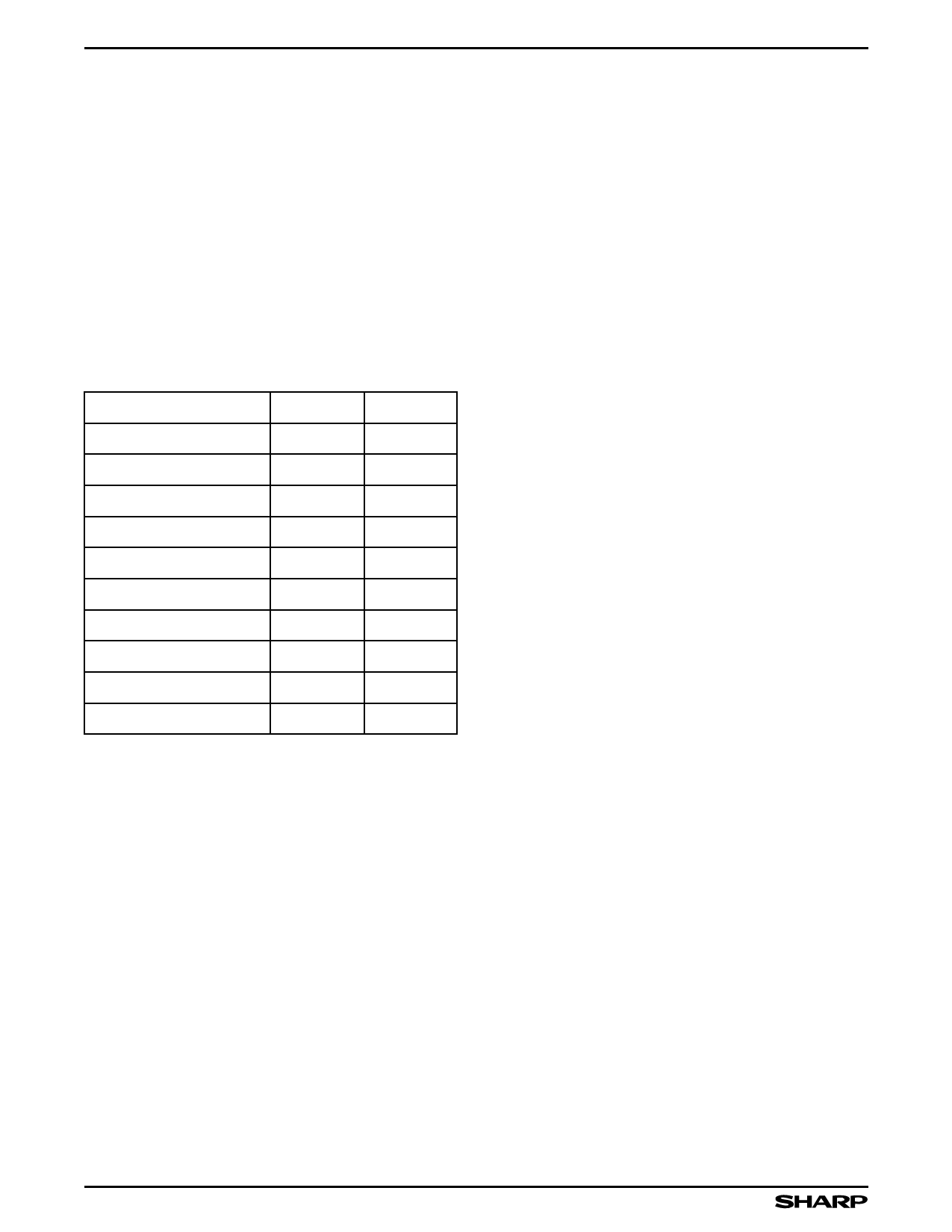
Identifier Codes
CODE
ADDRESS
DATA
Manufacturer Code
00000
89
Device Code
00001
A6
Block Lock Configurations X00021
ΓÇó Block is Unlocked
ΓÇó Block is Locked
ΓÇó Reserved for Future Use
Master Lock Configuration
00003
DQ0 = 0
DQ0 = 1
DQ1 - DQ7
ΓÇó Device is Unlocked
ΓÇó Device is Locked
ΓÇó Reserved for Future Use
DQ0 = 0
DQ0 = 1
DQ1 - DQ7
NOTE:
1. X selects the specific block lock configuration code to be read.
See Figure 5 for the device identifier code memory map.
Read Status Register Command
The status register may be read to determine when
a block erase, byte write, or lock-bit configuration is com-
plete and whether the operation completed success-
fully. It may be read at any time by writing the Read
Status Register command. After writing this command,
all subsequent read operations output data from the
status register until another valid command is written.
The status register contents are latched on the falling
edge of OE ┬╗ or CE ┬╗, whichever occurs. OE ┬╗ or CE ┬╗ must
toggle to VIH before further reads to update the status
register latch. The Read Status Register command func-
tions independently of the VPP voltage. RP ┬╗ can be VIH
or VHH.
Clear Status Register Command
Status register bits SR.5, SR.4, SR.3 and SR.1 are
set to '1' by the WSM and can only be reset by the Clear
Status Register command. These bits indicate various
failure conditions (see Status Register). By allowing sys-
tem software to reset these bits, several operations
(such as cumulatively erasing or locking multiple blocks
or writing several bytes in sequence) may be performed.
The status register may be polled to determine if an
error occurred during the sequence.
To clear the status register, the Clear Status Regis-
ter command (50H) is written. It functions independently
of the applied VPP Voltage. RP ┬╗ can be VIH or VHH. This
command is not functional during block erase or byte
write suspend modes.
Block Erase Command
Erase is executed one block at a time and initiated
by a two-cycle command. A block erase setup is first
written, followed by a block erase confirm. This com-
mand sequence requires appropriate sequencing and
an address within the block to be erased (erase changes
all block data to FFH). Block preconditioning, erase, and
verify are handled internally by the WSM (invisible to
the system). After the two-cycle block erase sequence
is written, the device automatically outputs status reg-
ister data when read (see Figure 6). The CPU can
detect block erase completion by analyzing the output
data of the RY ┬╗/BY ┬╗ or status register bit SR.7.
When the block erase is complete, status register bit
SR.5 should be checked. If a block erase error is
detected, the status register should be cleared before
system software attempts corrective actions. The CUI
remains in read status register mode until a new com-
mand is issued.
This two-step command sequence of set-up followed
by execution ensures that block contents are not acci-
dentally erased. An invalid Block Erase command
sequence will result in both status register bits
SR.4 and SR.5 being set to '1'. Also, reliable block era-
sure can only occur when VCC = VCC1/2/3 and
VPP = VPPH1/2/3. In the absence of this high voltage,
block contents are protected against erasure. If block
erase is attempted while VPP Γë¨ VPPLK, SR.3 and SR.5
will be set to '1'. Successful block erase requires that
the corresponding block lock-bit be cleared or, if set,
that RP ┬╗ = VHH. If block erase is attempted when the
corresponding block lock-bit is set and RP ┬╗ = VIH, SR.1
and SR.5 will be set to '1'. Block erase operations with
VIH < RP ┬╗ < VHH produce spurious results and should
not be attempted.
10
Share Link: 