LH28F008SC View Datasheet(PDF) - Sharp Electronics
Part Name
Description
Manufacturer
LH28F008SC Datasheet PDF : 38 Pages
| |||
8M (1M √ó 8) Flash Memory
LH28F008SC
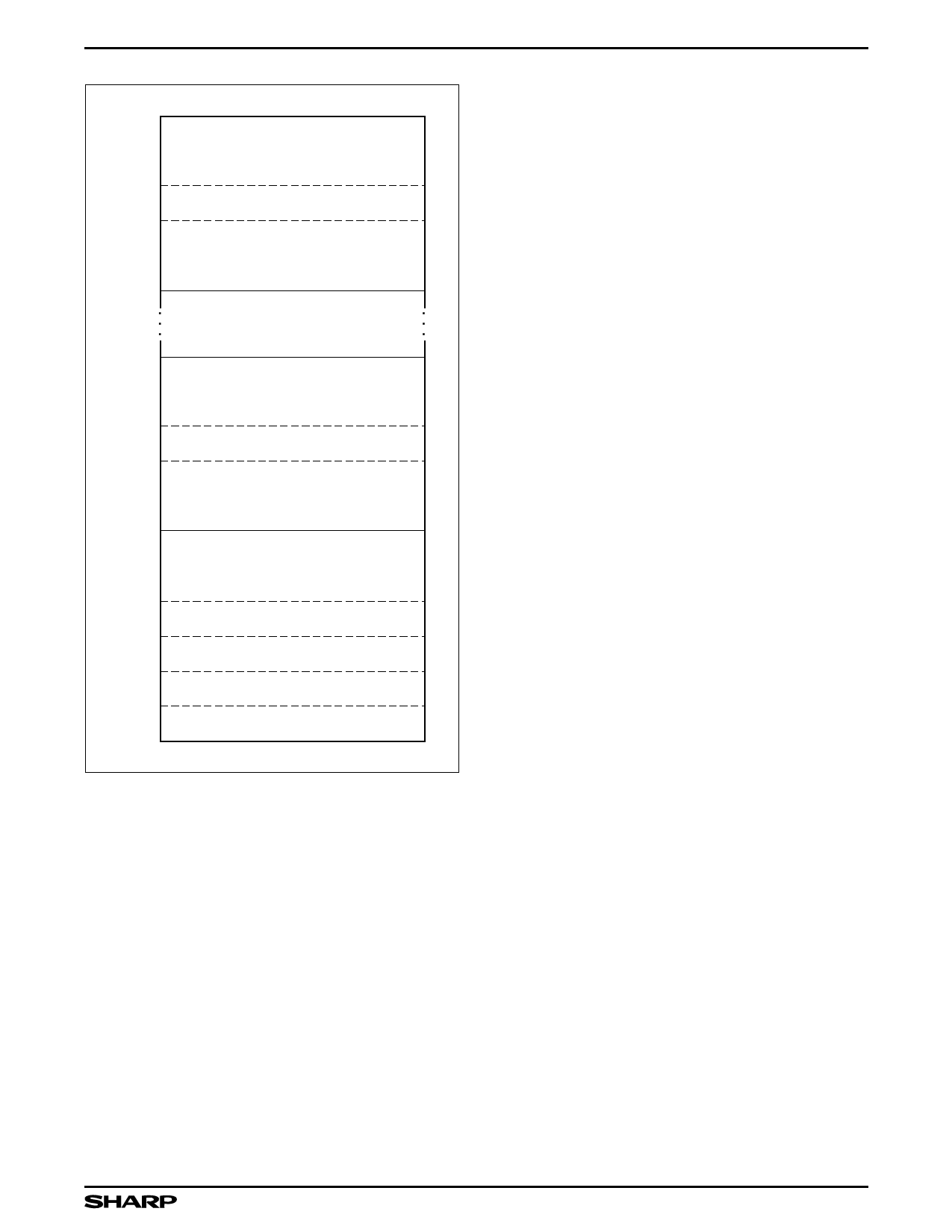
FFFFF
F0004
F0003
RESERVED FOR
FUTURE IMPLEMENTATION
F0002 BLOCK 15 LOCK CONFIGURATION CODE
F0001
F0000
RESERVED FOR
FUTURE IMPLEMENTATION
BLOCK 15
(BLOCKS 2 THROUGH 14)
1FFFF
10004
10003
10002
10001
10000
0FFFF
00004
00003
RESERVED FOR
FUTURE IMPLEMENTATION
BLOCK 1 LOCK CONFIGURATION CODE
RESERVED FOR
FUTURE IMPLEMENTATION
BLOCK 1
RESERVED FOR
FUTURE IMPLEMENTATION
MASTER LOCK CONFIGURATION CODE
00002 BLOCK 0 LOCK CONFIGURATION CODE
00001
DEVICE CODE
00000
MANUFACTURER CODE BLOCK 0
28F008SC-5
Figure 5. Device Identifier Code Memory Map
Write
Writing commands to the CUI enable reading of
device data and identifier codes. They also control
inspection and clearing of the status register. When
VPP = VPPH1/2/3, the CUI additionally controls block era-
sure, byte write, and lock-bit configuration.
The Block Erase command requires appropriate com-
mand data and an address within the block to be erased.
The Byte Write command requires the command and
address of the location to be written. Set Master and
Block Lock-Bit commands require the command and
address within the device (Master Lock) or block within
the device (Block Lock) to be locked. The Clear Block
Lock-Bits command requires the command and address
within the device.
The CUI does not occupy an addressable memory
location. It is written when WE » and CE » are active. The
address and data needed to execute a command are
latched on the rising edge of WE » or CE » (whichever
goes high first). Standard microprocessor write timings
are used. Figures 16 and 17 illustrateWE » and CE » con-
trolled write operations.
COMMAND DEFINITIONS
When the VPP voltage ≤ VPPLK, Read operations
from the status register, identifier codes, or blocks are
enabled. Placing VPPH1/2/3 on VPP enables successful
block erase, byte write and lock-bit configuration
operations.
Device operations are selected by writing specific
commands into the CUI.The Command DefinitionsTable
defines these commands.
Read Array Command
Upon initial device power-up and after exit from deep
power-down mode, the device defaults to read array
mode. This operation is also initiated by writing the Read
Array command. The device remains enabled for reads
until another command is written. Once the internal
WSM has started a block erase, byte write or lock-bit
configuration, the device will not recognize the Read
Array command until the WSM completes its operation
unless the WSM is suspended via an Erase Suspend
or Byte Write Suspend command.The Read Array com-
mand functions independently of the VPP voltage and
RP » can be VIH or VHH.
7
Share Link: 