LT3971AIMSE-TRPBF View Datasheet(PDF) - Linear Technology
Part Name
Description
Manufacturer
LT3971AIMSE-TRPBF Datasheet PDF : 24 Pages
| |||
LT3971A/LT3971A-5
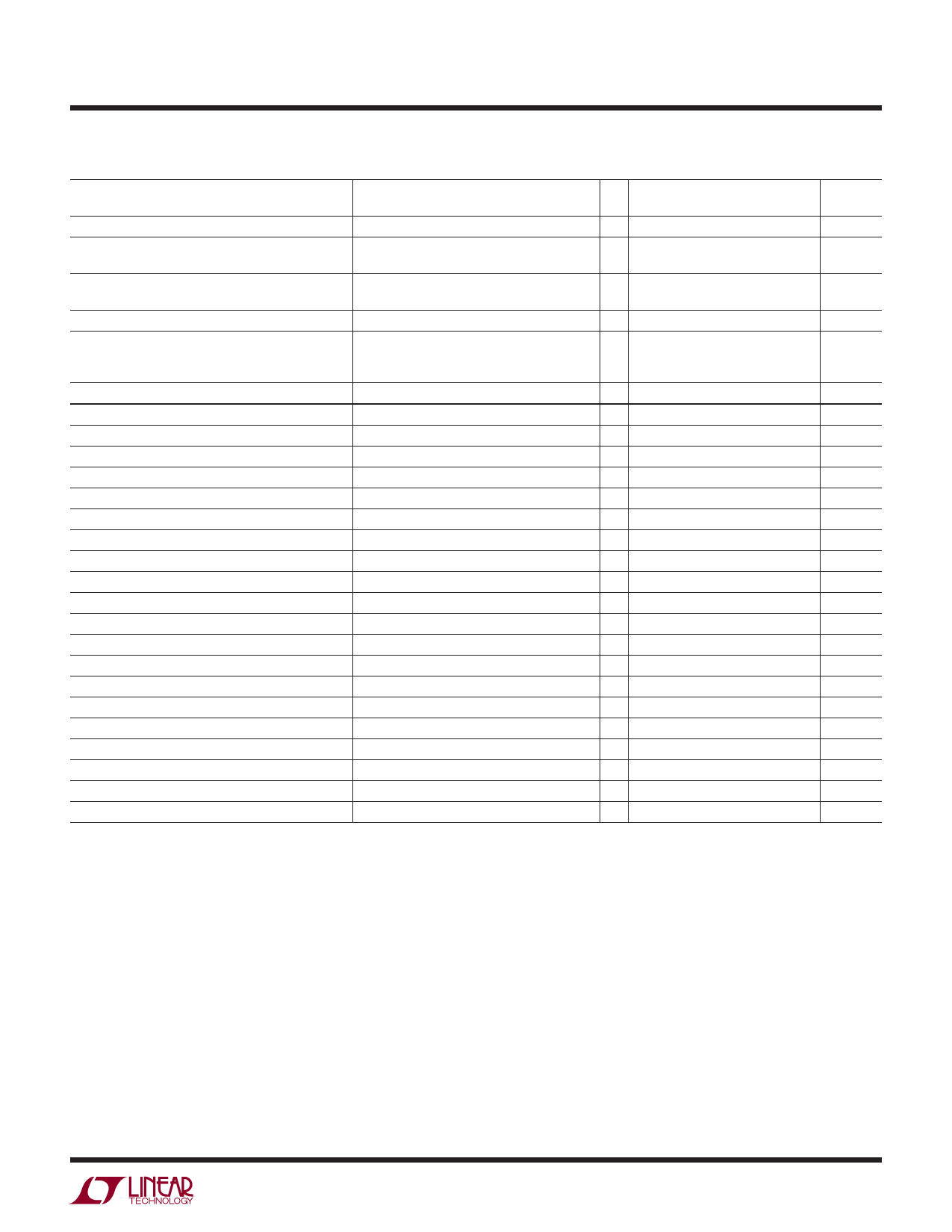
ELECTRICAL CHARACTERISTICS The l denotes the specifications which apply over the full operating
temperature range, otherwise specifications are at TA = 25°C. VIN = 12V, VEN = 12V, VBD = 3.3V unless otherwise noted. (Note 2)
VOUT Pin Current
VOUT Pin Clamp Voltage
Feedback Voltage
LT3971A-5 Output Voltage
FB Voltage Line Regulation
Switching Frequency
Minimum Switch On Time
Minimum Switch Off Time
Switch Current Limit
Switch VCESAT
Switch Leakage Current
Boost Schottky Forward Voltage
Boost Schottky Reverse Leakage
Minimum Boost Voltage (Note 3)
BOOST Pin Current
EN Voltage Threshold
EN Voltage Hysteresis
EN Pin Current
LT3971A PG Threshold Offset from VFB
LT3971A PG Hysteresis
LT3971A-5 PG Threshold Offset from VOUT
LT3971A-5 PG Hysteresis
PG Leakage
PG Sink Current
SYNC Threshold
SYNC Pin Current
SS Source Current
VOUT = 5V
VOUT = 5V
IVOUT = –2mA
4.3V < VIN < 38V (Note 4)
RT = 11k
RT = 35.7k
RT = 255k
ISW = 1A
ISH = 100mA
VREVERSE = 12V
VIN = 5V
ISW = 1A, VBOOST = 15V
EN Rising
VFB Rising
VOUT Rising
VPG = 3V
VPG = 0.4V
VSS = 1V
–0.65
–0.5
–0.38
μA
l –0.90
–0.5
–0.32
μA
9
11
13
V
1.176 1.192 1.204
V
l 1.173
1.19
1.207
V
4.94
5.01
5.06
V
l 4.93
5
5.07
V
0.0002 0.01
%/V
1.8
2.2
2.6
MHz
0.8
1
1.2
MHz
160
200
240
kHz
80
ns
110
150
ns
2.0
2.5
3.2
A
330
mV
0.02
1
μA
770
mV
0.02
1
μA
l
1.4
1.8
V
20
28
mA
l 0.95
1.01
1.07
V
30
mV
0.2
20
nA
60
100
140
mV
20
mV
5.5
9
12.5
%
1.3
%
0.02
1
μA
l 300
570
μA
0.6
0.8
1.0
V
0.1
nA
0.6
1
1.6
μA
Note 1: Stresses beyond those listed under Absolute Maximum Ratings
may cause permanent damage to the device. Exposure to any Absolute
Maximum Rating condition for extended periods may affect device
reliability and lifetime.
Note 2: The LT3971AI is guaranteed over the full –40°C to 125°C operating
junction temperature range. High junction temperatures degrade operating
lifetimes. Operating lifetime is derated at junction temperatures greater
than 125°C.
Note 3: This is the minimum voltage across the boost capacitor needed to
guarantee full saturation of the switch.
Note 4: Minimum input voltage depends on application circuit.
3971af
3
Share Link: 