LTC2362HS6 View Datasheet(PDF) - Linear Technology
Part Name
Description
Manufacturer
LTC2362HS6 Datasheet PDF : 20 Pages
| |||
LTC2360/LTC2361/LTC2362
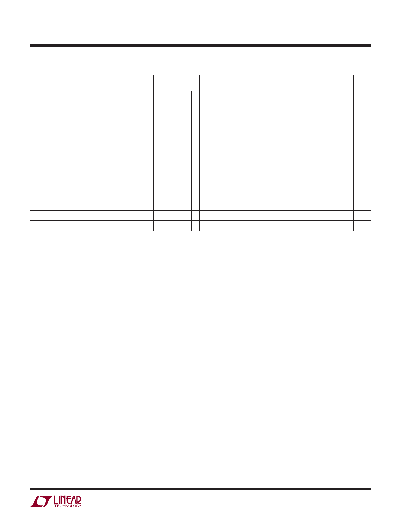
TIMING CHARACTERISTICS The l denotes the specifications which apply over the full operating temperature
range, otherwise specifications are at TA = 25°C. (Note 4)
SYMBOL PARAMETER
CONDITIONS
LTC2360
MIN TYP MAX
fSMPL(MAX) Maximum Sampling Frequency
(Notes 8, 9) l 100
fSCK
Shift Clock Frequency
(Notes 8, 9) l
10
tSCK
Shift Clock Period
l 100
tTHROUGHPUT Minimum Throughput Time, tACQ + tCONV
l
10
tACQ
Acquisition Time
l2
tCONV
Conversion Time
l8
t1
Minimum Positive CONV Pulse Width (Note 8)
l8
t2
SCK↑ Setup Time After CONV↓
(Note 8)
l 16
t3
SDO Enabled Time After CONV↓
(Notes 8, 9) l
16
t4
SDO Data Valid Access Time After SCK↓ (Notes 8, 9, 10) l
8
t5
SCK Low Time
(Note 11)
l 40%
t6
SCK High Time
(Note 11)
l 40%
t7
SDO Data Valid Hold Time After SCK↓ (Notes 8, 9, 10) l 4
t8
SDO Into Hi-Z State Time After CONV↑ (Notes 8, 9)
6
LTC2361
MIN TYP MAX
250
25
40
4
1
3
3
16
16
8
40%
40%
4
6
LTC2362
MIN TYP MAX
500
50
20
2
0.5
1.5
1.5
16
16
8
40%
40%
4
6
UNITS
kHz
MHz
ns
μs
μs
μs
μs
ns
ns
ns
tSCK
tSCK
ns
ns
Note 1: Stresses beyond those listed under Absolute Maximum Ratings
may cause permanent damage to the device. Exposure to any Absolute
Maximum Rating condition for extended periods may affect device
reliability and lifetime.
Note 2: All voltage values are with respect to GND.
Note 3: When pins AIN and VREF are taken below GND or above VDD,
they will be clamped by internal diodes. These products can handle input
currents greater than 100mA below GND or above VDD without latch-up.
Note 4: VDD = OVDD = VREF = 2.35V to 3.6V, fSMPL = fSMPL(MAX) and
fSCK = fSCK(MAX) unless otherwise specified.
Note 5: Integral linearity is defined as the deviation of a code from a
straight line passing through the actual endpoints of the transfer curve.
The deviation is measured from the center of the quantization band.
Note 6: Linearity, offset and gain specifications apply for a single-ended
AIN input with respect to GND.
Note 7: Typical RMS noise at code transitions.
Note 8: Guaranteed by characterization. All input signals are specified with
tr = tf = 2ns (10% to 90% of VDD) and timed from a voltage level of 1.6V.
Note 9: All timing specifications given are with a 10pF capacitance load.
With a capacitance load greater than this value, a digital buffer or latch
must be used.
Note 10: The time required for the output to cross the VIH or VIL voltage.
Note 11: Guaranteed by design, not subject to test.
Note 12: High temperatures degrade operating lifetimes. Operating lifetime
is derated at temperatures greater than 105°C.
236012fa
5
Share Link: 