LH28F020SU-N View Datasheet(PDF) - Sharp Electronics
Part Name
Description
Manufacturer
LH28F020SU-N Datasheet PDF : 31 Pages
| |||
2M (256K √ó 8) Flash Memory
LH28F020SU-N
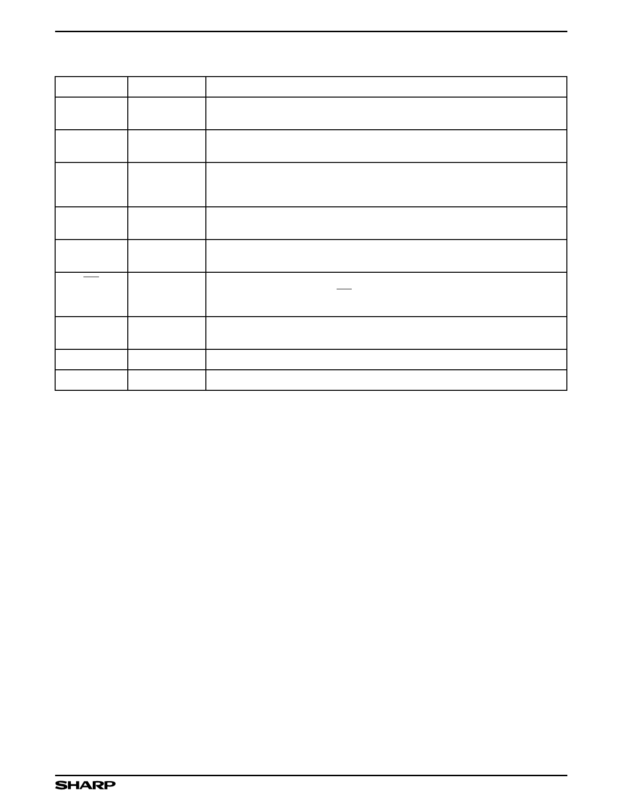
PIN DESCRIPTION
SYMBOL
A0 - A13
A14 - A17
DQ0 - DQ7
CE »
OE »
WE
VP P
VC C
GND
TYPE
NAME AND FUNCTION
INPUT
BYTE-SELECT ADDRESSES: Select a byte within one 16K block. These
addresses are latched during Data Writes.
INPUT
BLOCK-SELECT ADDRESSES: Select 1 of 16 Erase Blocks. These addresses are
latched during Data Writes, Erase and Lock-Block operations.
INPUT/OUTPUT DATA INPUT/OUTPUT: Inputs data and commands during CUI write cycles.
Outputs array, buffer, identifier or status data in the appropriate Read mode.
Floated when the chip is de-selected or the outputs are disabled.
INPUT
CHIP ENABLE INPUTS: Activate the device's control logic, input buffers, decoders
and sense amplifiers. CE » must be low to select the device.
INPUT
OUTPUT ENABLE: Gates device data through the output buffers when low. The
outputs float to tri-state off when OE» is high.
INPUT
WRITE ENABLE: Controls access to the CUI, Page Buffers, Data Queue Registers
and Address Queue Latches. WE is active low, and latches both address and data
(command or array) on its rising edge.
SUPPLY
ERASE/WRITE POWER SUPPLY (5.0 V ±0.5 V): For erasing memory array blocks
or writing words/bytes/pages into the flash array.
SUPPLY
DEVICE POWER SUPPLY (5.0 V ±0.5 V): Do not leave any power pins floating.
SUPPLY
GROUND FOR ALL INTERNAL CIRCUITRY: Do not leave any ground pins floating.
INTRODUCTION
Sharp’s LH28F020SU-N 2M Flash Memory is a revo-
lutionary architecture which enables the design of truly
mobile, high performance, personal computing and com-
munication products. With innovative capabilities, 5.0V
single voltage operations and very high read/write per-
formance, the LH28F020SU-N is also the ideal choice
for designing embedded mass storage flash memory
systems.
The LH28F020SU-N is a very high density, highest
performance non-volatile read/write solution for solid-
state storage applications. Its independently lockable
16 symmetrical blocked architecture (16K each)
extended cycling, low power operation, very fast write
and read performance and selective block locking pro-
vide a highly flexible memory component suitable for
high density memory cards, Resident Flash Arrays and
PCMCIA-ATA Flash Drives. The LH28F020SU-N single
voltage power supply operation enables the design of
memory cards which can be read/written in 5.0 V sys-
tems. Its x8 architecture allows the optimization of
memory to processor interface. The flexible block lock-
ing option enables bundling of executable application
software in a Resident Flash Array or memory card.
Manufactured on Sharp’s 0.55 µm ETOX™ process
technology, the LH28F020SU-N is the most cost-
effective, high density 5.0 V flash memory.
Description
The LH28F020SU-N is a high performance 2M
(2,097,152 bit) block erasable non-volatile random
access memory organized as 256K √ó 8. The
LH28F020SU-N includes sixteen 16K (16,384) blocks.
A chip memory map is shown in Figure 4.
The implementation of a new architecture, with many
enhanced features, will improve the device operating
characteristics and results in greater product reliability
and ease of use.
Among the significant enhancements of the
LH28F020SU-N80:
• 5 V Read, Write/Erase Operation
(5 V VCC, 5.0 V VPP)
• Lower Power Capability
• Improved Write Performance
• Dedicated Block Write/Erase Protection
• Command-Controlled Memory Protection
Set/Reset Capability
The LH28F020SU-N will be available in a 32-pin,
525 mil. SOP package. This form factor and pinout al-
low for very high board layout densities.
3
Share Link: 