AT89LP4052(2008) View Datasheet(PDF) - Atmel Corporation
Part Name
Description
Manufacturer
AT89LP4052 Datasheet PDF : 93 Pages
| |||
AT89LP2052/LP4052
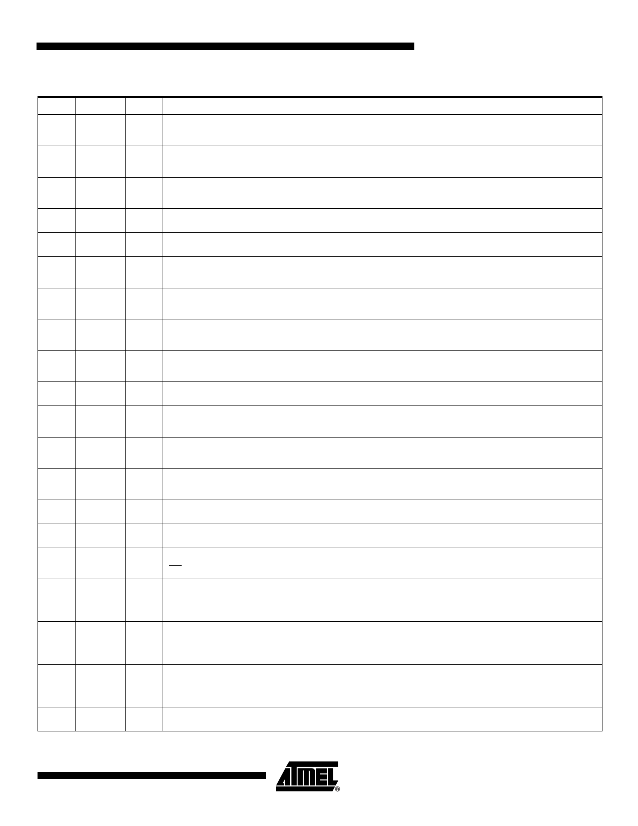
3. Pin Description
Pin Symbol Type Description
I RST: External Active-High Reset input.
1
RST
I VPP: Parallel Programming Voltage. Raise to 12V to enable programming.
I/O P3.0: User-configurable I/O Port 3 bit 0.
2
P3.0
I RXD: Serial Port Receiver input.
I/O P3.1: User-configurable I/O Port 3 bit 1.
3
P3.1
O TXD: Serial Port Transmitter output.
4
XTAL2
O XTAL2: Output from inverting oscillator amplifier.
5
XTAL1
I XTAL1: Input to the inverting oscillator amplifier and internal clock generation circuits.
I/O P3.2: User-configurable I/O Port 3 bit 2.
6
P3.2
I INT0: External Interrupt 0 input.
I/O P3.3: User-configurable I/O Port 3 bit 3.
7
P3.3
I INT1: External Interrupt 1input.
I/O P3.4: User-configurable I/O Port 3 bit 4.
8
P3.4
I/O T0: Timer 0 Counter input or PWM output
I/O P3.5: User-configurable I/O Port 3 bit 5.
9
P3.5
I/O T1: Timer 1 Counter input or PWM output
10
GND
I Ground
I/O P3.7: User-configurable I/O Port 3 bit 7.
11
P3.7
O SYSCLK: System Clock Output when System Clock Fuse is enabled.
I/O P1.0: User-configurable I/O Port 1 bit 0.
12
P1.0
I AIN0: Analog Comparator Positive input.
I/O P1.1: User-configurable I/O Port 1 bit 1.
13
P1.1
I AIN1: Analog Comparator Negative input.
14
P1.2
I/O P1.2: User-configurable I/O Port 1 bit 2.
15
P1.3
I/O P1.3: User-configurable I/O Port 1 bit 3
I/O P1.4: User-configurable I/O Port 1 bit 4.
16
P1.4
I SS: SPI slave select.
I/O P1.5: User-configurable I/O Port 1 bit 5.
17
P1.5
I/O
MOSI: SPI master-out/slave-in. When configured as master, this pin is an output. When configured as
slave, this pin is an input.
I/O P1.6: User-configurable I/O Port 1 bit 6.
18
P1.6
I/O
MISO: SPI master-in/slave-out. When configured as master, this pin is an input. When configured
as slave, this pin is an output.
I/O P1.7: User-configurable I/O Port 1 bit 7.
19
P1.7
I/O
SCK: SPI Clock. When configured as master, this pin is an output. When configured as slave, this pin is
an input.
20
VCC
I Supply Voltage
3
3547I–MICRO–6/08
Share Link: 