ESD5Z12T1G(2012) View Datasheet(PDF) - ON Semiconductor
Part Name
Description
Manufacturer
ESD5Z12T1G Datasheet PDF : 5 Pages
| |||
ESD5Z2.5T1G Series, SZESD5Z2.5T1G Series
MAXIMUM RATINGS
Rating
Symbol
Value
Unit
IEC 61000−4−2 (ESD)
Contact
Air
kV
30
30
IEC 61000−4−4 (EFT)
40
A
ESD Voltage
Per Human Body Model
Per Machine Model
kV
16
V
400
Total Power Dissipation on FR−5 Board (Note 1) @ TA = 25C
PD
200
mW
Junction and Storage Temperature Range
TJ, Tstg
−55 to +150
C
Lead Solder Temperature − Maximum (10 Second Duration)
TL
260
C
Stresses exceeding Maximum Ratings may damage the device. Maximum Ratings are stress ratings only. Functional operation above the
Recommended Operating Conditions is not implied. Extended exposure to stresses above the Recommended Operating Conditions may affect
device reliability.
1. FR−5 = 1.0 x 0.75 x 0.62 in.
See Application Note AND8308/D for further description of survivability specs.
ELECTRICAL CHARACTERISTICS
(TA = 25C unless otherwise noted)
Symbol
Parameter
IPP
Maximum Reverse Peak Pulse Current
VC
Clamping Voltage @ IPP
VRWM Working Peak Reverse Voltage
IR
Maximum Reverse Leakage Current @ VRWM
VBR Breakdown Voltage @ IT
IT
Test Current
IF
Forward Current
VF
Forward Voltage @ IF
Ppk
Peak Power Dissipation
C
Max. Capacitance @VR = 0 and f = 1 MHz
*See Application Note AND8308/D for detailed explanations of
datasheet parameters.
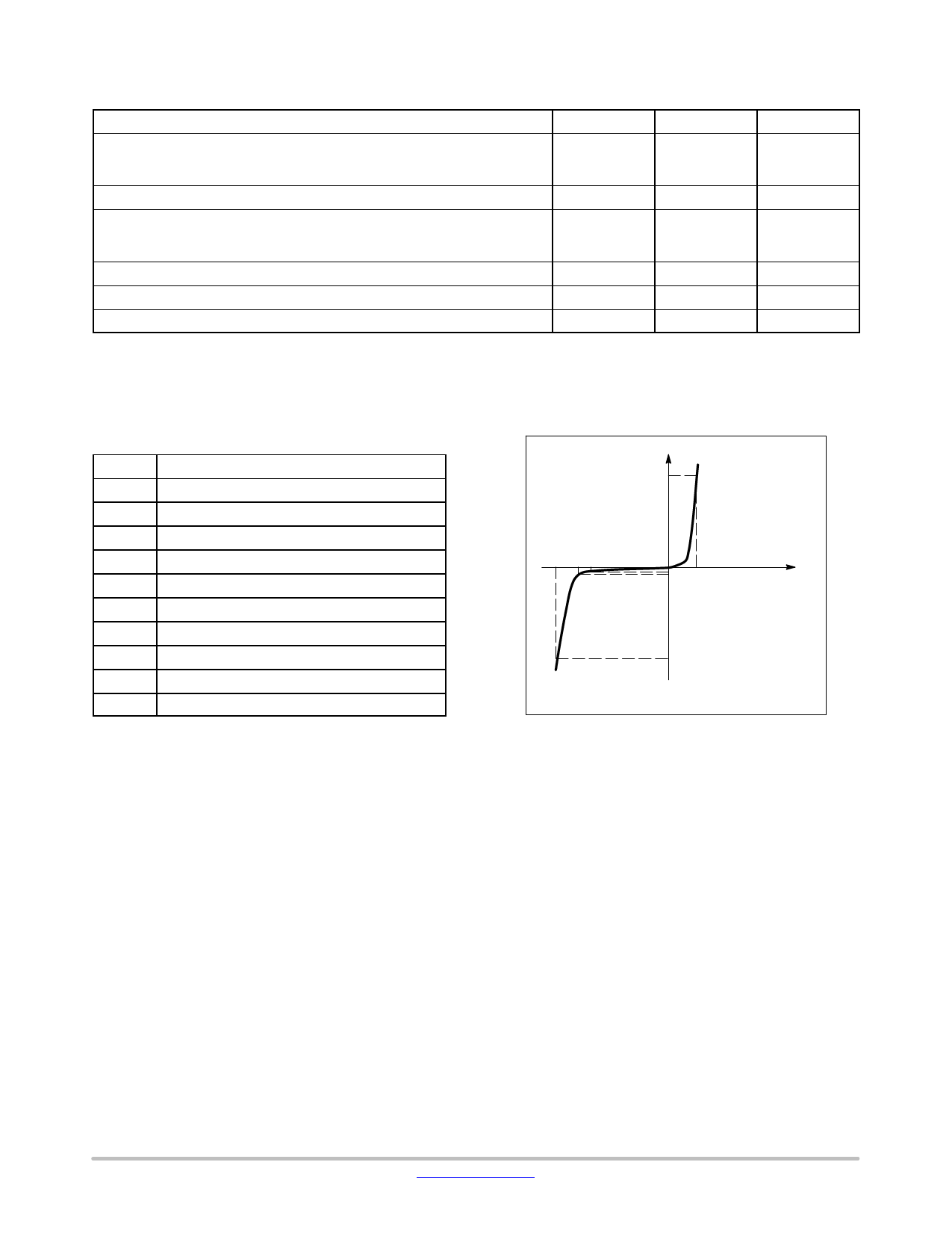
I
IF
VC VBR VRWM
IIRT VF
V
IPP
Uni−Directional TVS
http://onsemi.com
2
Share Link: 