98ASH70169A View Datasheet(PDF) - NXP Semiconductors.
Part Name
Description
Manufacturer
98ASH70169A Datasheet PDF : 37 Pages
| |||
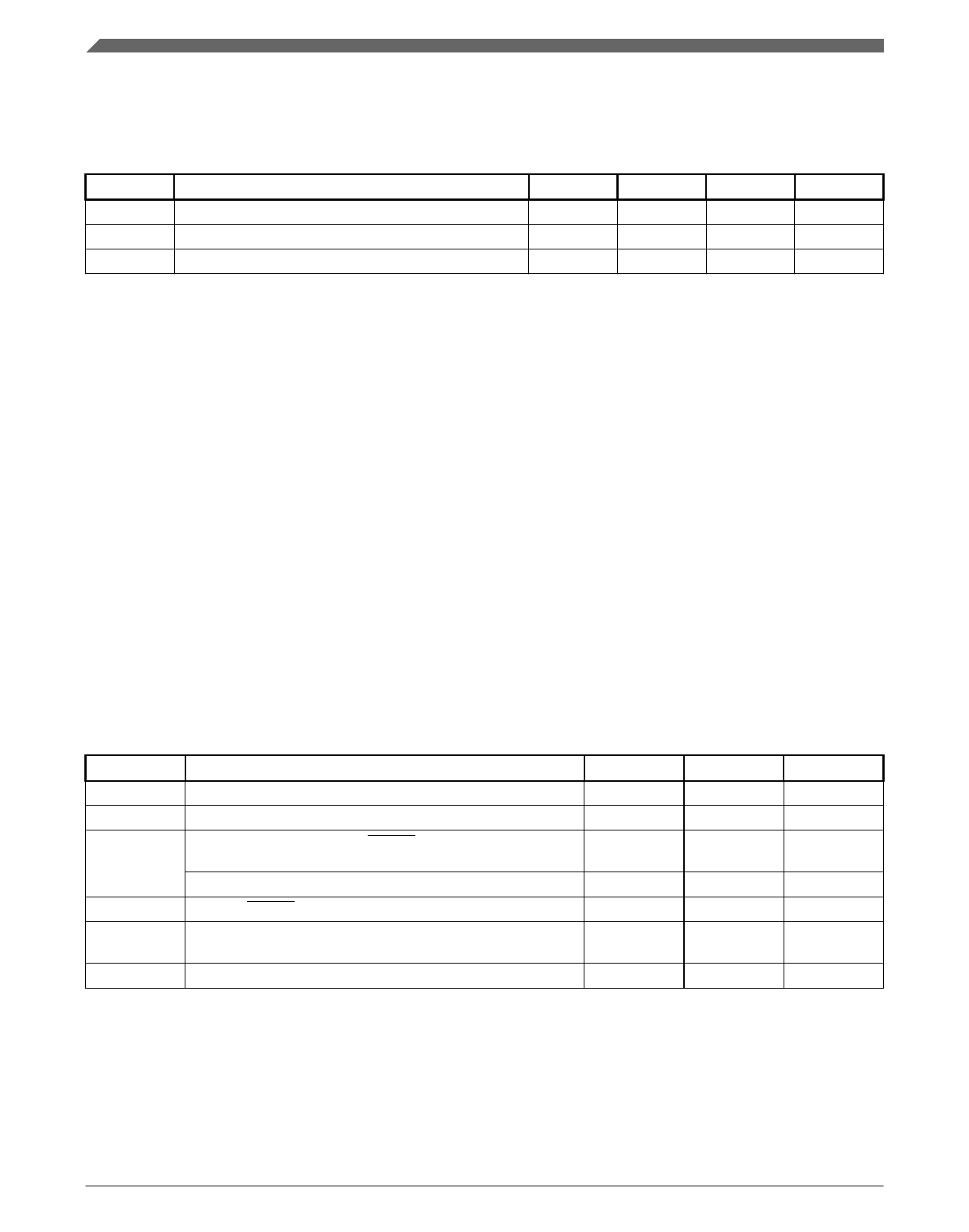
Ratings
5.3 ESD handling ratings
Symbol
VHBM
VCDM
ILAT
Description
Electrostatic discharge voltage, human body model
Electrostatic discharge voltage, charged-device model
Latch-up current at ambient temperature of 105 °C
Min.
-6000
-500
-100
Max.
+6000
+500
+100
Unit
V
V
mA
Notes
1
2
1. Determined according to JEDEC Standard JESD22-A114, Electrostatic Discharge (ESD) Sensitivity Testing Human Body
Model (HBM).
2. Determined according to JEDEC Standard JESD22-C101, Field-Induced Charged-Device Model Test Method for
Electrostatic-Discharge-Withstand Thresholds of Microelectronic Components.
5.4 Voltage and current operating ratings
Absolute maximum ratings are stress ratings only, and functional operation at the
maxima is not guaranteed. Stress beyond the limits specified in below table may affect
device reliability or cause permanent damage to the device. For functional operating
conditions, refer to the remaining tables in this document.
This device contains circuitry protecting against damage due to high static voltage or
electrical fields; however, it is advised that normal precautions be taken to avoid
application of any voltages higher than maximum-rated voltages to this high-impedance
circuit. Reliability of operation is enhanced if unused inputs are tied to an appropriate
logic voltage level (for instance, either VSS or VDD) or the programmable pullup resistor
associated with the pin is enabled.
Symbol Description
Min.
Max.
Unit
VDD
Supply voltage
–0.3
6.0
V
IDD
Maximum current into VDD
—
120
mA
VDIO
Digital input voltage (except RESET, EXTAL, XTAL, or true
–0.3
VDD + 0.3
V
open drain pin PTA2 and PTA3)
Digital input voltage (true open drain pin PTA2 and PTA3)
-0.3
6
V
VAIO
Analog1, RESET, EXTAL, and XTAL input voltage
–0.3
VDD + 0.3
V
ID
Instantaneous maximum current single pin limit (applies to all
–25
25
mA
port pins)
VDDA
Analog supply voltage
VDD – 0.3
VDD + 0.3
V
1. All digital I/O pins, except open-drain pin PTA2 and PTA3, are internally clamped to VSS and VDD. PTA2 and PTA3 is only
clamped to VSS.
MC9S08PT16 Series Data Sheet, Rev. 4, 03/2020
8
NXP Semiconductors
Share Link: 