MCP1812A View Datasheet(PDF) - Microchip Technology
Part Name
Description
Manufacturer
MCP1812A
Microchip Technology

MCP1812A Datasheet PDF : 45 Pages
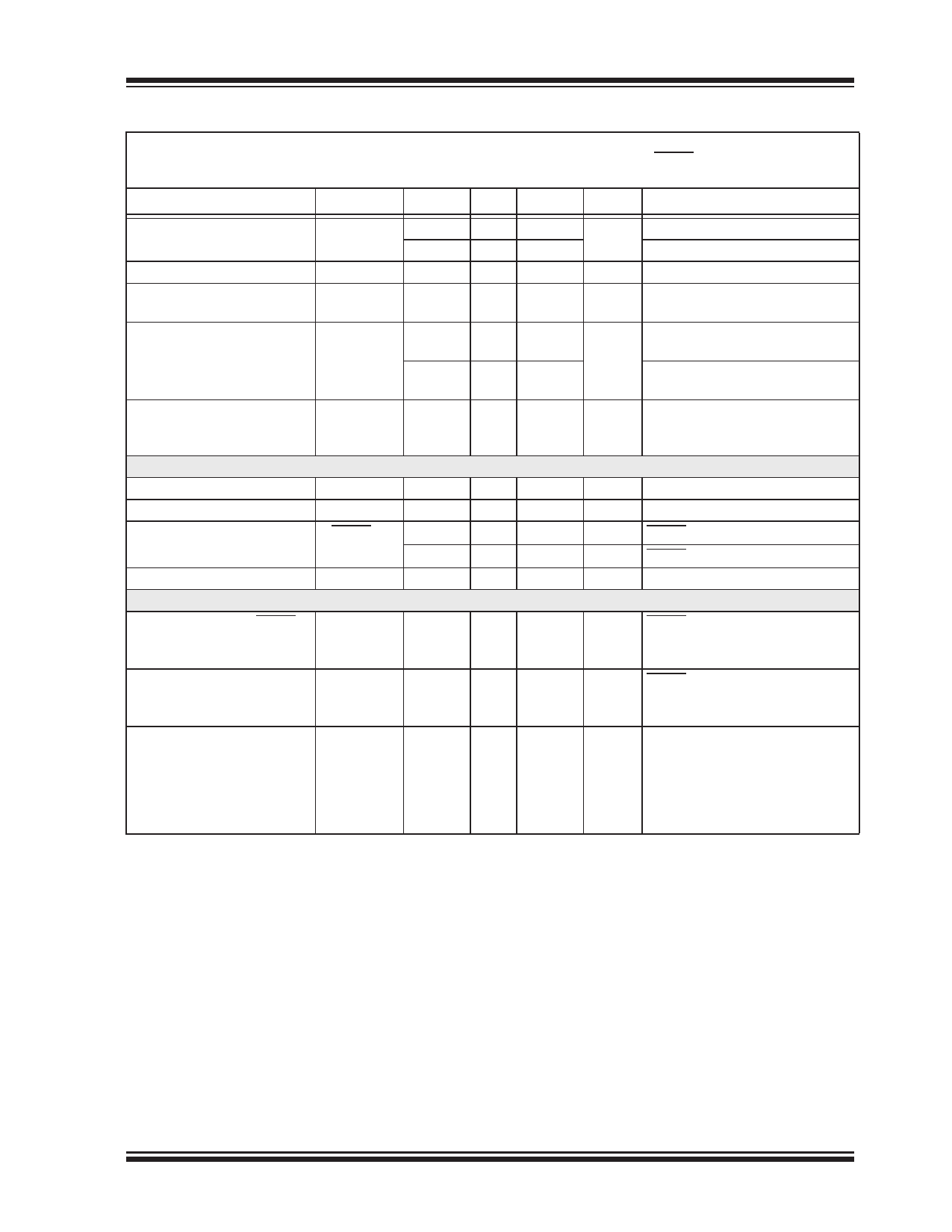
| |||
MCP1811A/11B/12A/12B
AC/DC CHARACTERISTICS (CONTINUED)
Electrical Specifications: Unless otherwise indicated, VIN = VR + 1V (Note 2), IOUT = 1 mA,
CIN = COUT = 1 μF (MCP1811X) or 2.2 μF (MCP1812X) ceramic (X7R), TA = +25°C, SHDN > 1.4V.
Boldface type applies for junction temperatures TJ of -40°C to +85°C (Note 4).
Parameters
Sym.
Min. Typ. Max. Units
Conditions
Foldback Current
Start-up Voltage Overshoot
Line Regulation
Load Regulation
VOVER
VOUT
VOUT
Dropout Voltage
VDROPOUT
Shutdown Input
Logic High Input
Logic Low Input
Shutdown Input Leakage
Current
Discharge Transistor RDCH
AC Performance
VSHDN-HIGH
VSHDN-LOW
SHDNILK
—
50
—
mA RLOAD = 1MCP1811X)
—
100
—
RLOAD = 1MCP1812X)
—
5
10 %VOUT VIN = 0V to 5.5V
—
±20
—
mV 1.8V < VIN < 5.5V (MCP1811X),
2.4V < VIN < 5.5V (MCP1812X)
—
±25
—
mV IOUT = 1 mA to 150 mA
(MCP1811X) (Note 3)
—
±50
—
IOUT = 1mA to 300 mA
(MCP1812X) (Note 3)
—
400 600
mV IOUT = 150 mA (MCP1811X),
IOUT = 300 mA (MCP1812X)
(Note 5)
70
—
—
%VIN
—
—
20
%VIN
— 0.100 0.500
nA SHDN = GND
—
1.0 20.0
nA SHDN = 5.5V
—
100
—
MCP1811A/12A
Start-up Delay from SHDN
Start-up Rise Time
Power Supply Ripple
Rejection Ratio
TDELAY
TRISE
PSRR
—
400
—
200
— 1000
—
-50
—
μs SHDN = GND to VIN,
VOUT = GND to 10%VR,
VIN = VR + 1V to 5.5V
μs SHDN = GND to VIN,
VOUT = 10%VR to 95% VR,
VIN = VR + 1V to 5.5V
dB CIN = 0 μF,
VIN = VR + 1V + VINAC/2 or
VIN = VIN_Min + 1V + VINAC/2,
IOUT = 10 mA and Full Load,
VINAC = 0.2Vpk-pk,
f = 1 kHz
1: The maximum allowable power dissipation is a function of ambient temperature, the maximum allowable
junction temperature and the thermal resistance from junction to air (i.e., TA, TJ, JA).
Exceeding the maximum allowable power dissipation will cause the operating junction temperature to exceed
the maximum +85°C rating. Sustained junction temperatures above +85°C can impact device reliability.
2: VR is a nominal regulator output voltage. The minimum VIN must meet two conditions: VIN ≥ VIN(MIN) and
VIN ≥ VR + VDROPOUT(MAX).
3: Load regulation is measured at a constant junction temperature using low duty cycle pulse testing. Load
regulation is tested over a load range from 1 mA to the maximum specified output current.
4: The junction temperature is approximated by soaking the device under test at an ambient temperature
equal to the desired Junction temperature. The test time is small enough such that the rise in the junction
temperature over the ambient temperature is not significant.
5: Dropout voltage is defined as the input-to-output voltage differential at which the output voltage drops 2%
below its nominal value that was measured with an input voltage of VIN = VR + 1V.
2018-2019 Microchip Technology Inc.
DS20006088B-page 5
Share Link: