HI-7159A View Datasheet(PDF) - Intersil
Part Name
Description
Manufacturer
HI-7159A Datasheet PDF : 14 Pages
| |||
HI-7159A
Serial Mode 1
Serial Mode 1 is selected by tying SMS0 (Pin 18) low, SMS1
(Pin 19) high, and SEL (Pin 28) low (Figure 4B). In this mode
the HI-7159A interface emulates a UART, reading and
writing data in serial data packets of 1 start bit, 8 data bits,
1 parity bit (EVEN), and 1 stop bit. The baud rate is
determined by the state of BRS0 and BRS1 (Pins 24 and 25)
as shown in Table 2. Pin 15 becomes the serial receiver pin
(RXD) and pin 16 the serial transmitter pin (TXD). CS (Pin
17) remains a chip select and must either be tied to DGND or
pulled low (see Figure 2B) to access the device.
SAD0-SAD3 (Pins 20-23) are unused in this mode and
should be tied high.
TABLE 2. BAUD RATE SELECTION FOR MODES 1 AND 2
BRS0
PIN 24
DGND
DGND
VCC
VCC
BRS1
PIN 25
DGND
VCC
DGND
VCC
BAUD RATE
(fXTAL = 2.4576MHz)
300
1200
9600
19200
BAUD RATE vs
fXTAL
fXTAL/8192
fXTAL/2048
fXTAL/256
fXTAL/128
-5V
+5V
µP
RD
WR
VEE
RD 14
15
WR
16
SEL
28
VCC
1
27
ADDRESS
BUS
DATA
ADDRESS
DECODER
D0
CS
17
D0
18
HI- 7159A
BUS
D7
25
D7
26
DGND
XTAL
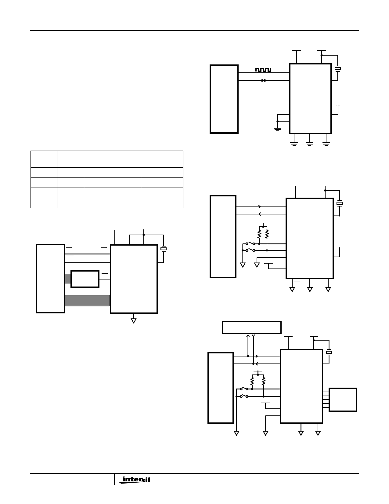
FIGURE 3. PARALLEL MODE CONFIGURATION
Design Hints for Operating in the Parallel
Mode
1. Always read the status byte twice to make sure that it is
cleared.
2. Make sure the status byte is cleared before issuing a
command to change modes.
3. Read each digit pair five times before reading the next
byte to ensure that the output data is correct.
4. Use a watchdog timer to monitor conversion time. If
conversion time is either too long or too short, reissue the
conversion command.
CLK
10
RXD/TXD
11
8051
µP
-5V
VEE
CLK 14
15
RXD/TXD
16
+5V
VCC
1
XTAL
27
XTAL
HI-7159A
+5V
SM0
SM1 18
19
17
20-25
26 28
CS DGND SEL
FIGURE 4A. SERIAL MODE 0
TXD
RXD
-5V
VEE
RXD 14
TXD 15
16
+5V
+5V
VCC
1
XTAL
27
XTAL
UART/µP
20K
20K
BRS0
24
BRS1 25
SM0 18
+5V
SM1 19
HI-7159A
+5V
20 - 23
17
26
28
CS
DGND SEL
FIGURE 4B. SERIAL MODE 1
TO UP TO 31 ADDITIONAL
HI-7159As
-5V
TXD
RXD
VEE
RXD 14
15
TXD
16
+5V
+5V
VCC
1
XTAL
27
XTAL
20K
UART/µP
20K
BRS0
24
BRS1
25
+5V
SM0
18
SM1 19
HI-7159A
20
21
22
23
17
ADDRESS
SELECT
26
28
DGND SEL
FIGURE 4C. SERIAL MODE 2
FIGURE 4. SERIAL MODE CONFIGURATIONS
7
Share Link: 