MC141540 View Datasheet(PDF) - Motorola => Freescale
Part Name
Description
Manufacturer
MC141540 Datasheet PDF : 12 Pages
| |||
DESIGN CONSIDERATIONS
Distortion
Motorola’s MC141540 has a built–in PLL for multi–system
application. Pin 2 voltage is dc–based for the internal VCO in
the PLL. When the input frequency (HFLB) to Pin 5 in-
creases, the VCO frequency will increase accordingly. This
forces the PLL to a higher locked frequency output. The fre-
quency should be equal to 320 x HFLB. This is the pixel dot
clock.
Display distortion is caused by noise on Pin 2. Positive
noise increases the VCO frequency above normal. The cor-
responding scan line will be shorter accordingly. In contrast,
negative noise causes the scan line to be longer. The net re-
sult will be distortion on the display, especially on the right
hand side of the display window.
In order to have distortion–free display, the following rec-
ommendations should be considered:
• Only analog part grounds (Pin 2 to Pin 4) can be con-
nected to Pin 1(VSS(A)). VSS and other grounds should be
connected to PCB common ground. The VSS(A) and VSS
grounds should be totally separated (i.e. VSS(A) is float-
ing). Refer to the Application Diagram for the ground con-
nections.
• The dc supply path for Pin 9 (VDD) should be separated
from other switching devices.
• The LC filter should be connected between Pin 9 and Pin
4. Refer to the values used in the Application Diagram.
• Biasing and filter networks should be connected to Pin 2
and Pin 3. Refer to the recommended networks in the Ap-
plication Diagram.
• Two small capacitors can be connected between Pins 2
and 3, and between Pins 3 and 4.
Jittering
Most display jittering is caused by HFLB jittering on Pin 5.
Care must be taken if the HFLB signal comes from the fly-
back transformer. A short path and shielded cable are rec-
ommended for a clean signal. A small capacitor can be
added between Pin 5 and Pin 16 to smooth the signal. Refer
to the value used in the Application Diagram.
Display Dancing
Most display dancing is caused by interference of the seri-
al bus. It can be avoided by adding series resistors to the se-
rial bus.
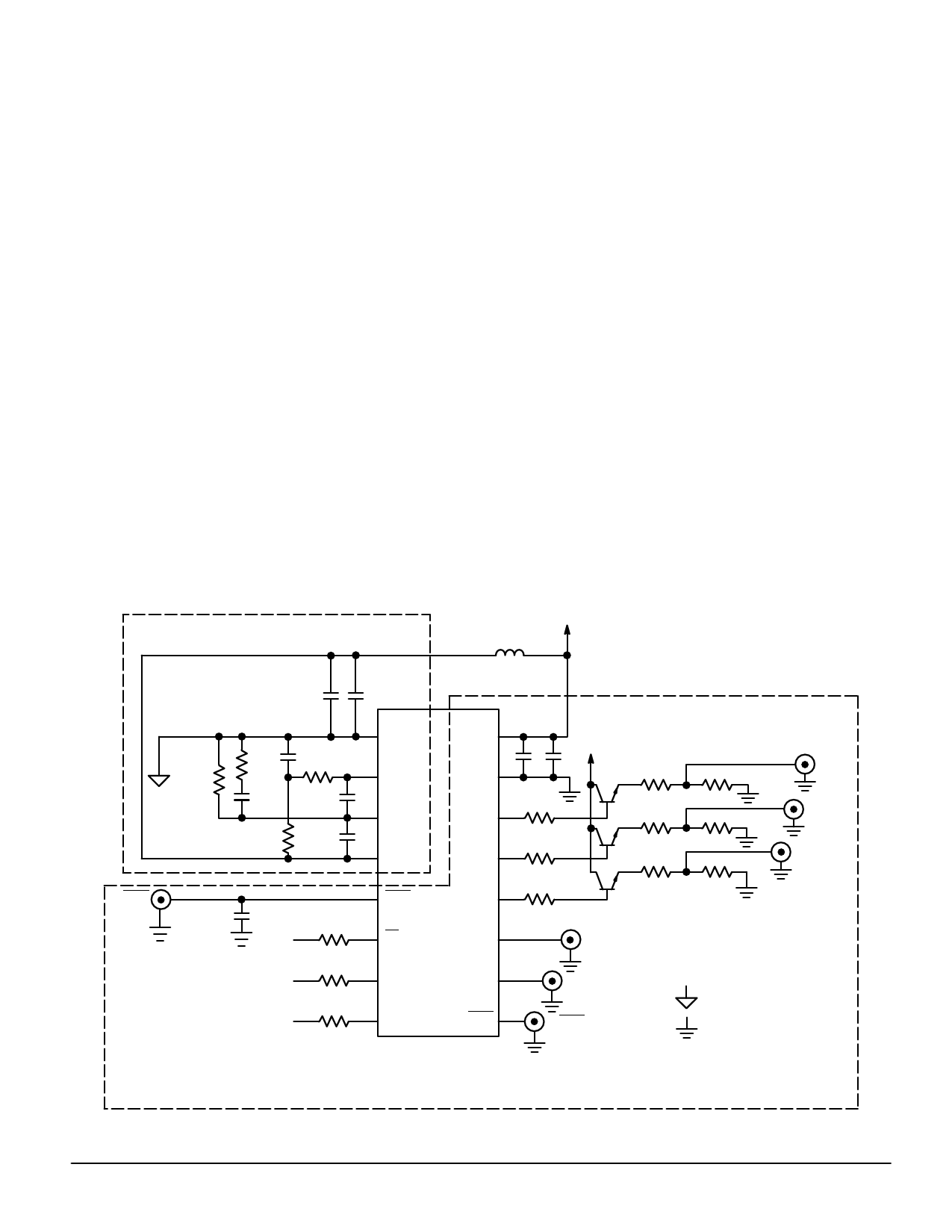
APPLICATION DIAGRAM
ANALOG GROUND – FLOATING
VCC
100 µH
HFLB
0.1 µF
0.01 µF
1k
2k
3.3 k
0.047
µF
33 pF
330 k 33 pF
330 pF
100
IIC(SPI) BUS
100
100
100 µF
1 VSS(A)
2 VCO
VDD 9
10 0.1 VCC
VSS 16 µF µF
240
3 RP
R 15 1 k
4 VDD(A)
14 1 k
G
5 HFLB
B 13 1 k
6
SS
MOSD
FBKG 12
240
240
MPS2369
FBKG
7
SDA(MOSI)
HTONE 11
HTONE
8
SCL(SCK)
VFLB 10
VFLB
100
R
100
G
100
B
ANALOG GROUND
DIGITAL GROUND
DIGITAL GROUND – COMMON GROUND
MOTOROLA
MC141540
11
Share Link: 