MC141540 View Datasheet(PDF) - Motorola => Freescale
Part Name
Description
Manufacturer
MC141540 Datasheet PDF : 12 Pages
| |||
ABSOLUTE MAXIMUM RATINGS Voltage Referenced to VSS
Symbol
Characteristic
Value
Unit
VDD Supply Voltage
– 0.3 to + 7.0
V
Vin Input Voltage
VSS – 0.3 to
V
VDD + 0.3
Id
Current Drain per Pin Excluding VDD
and VSS
25
mA
Ta
Operating Temperature Range
0 to 85
°C
Tstg Storage Temperature Range
– 65 to + 150
°C
NOTE: Maximum Ratings are those values beyond which damage to the device may occur.
Functional operation should be restricted to the limits in the Electrical Characteris-
tics tables or Pin Description section.
This device contains circuitry to protect the
inputs against damage due to high static volt-
ages or electric fields; however, it is advised that
normal precautions be taken to avoid applica-
tions of any voltage higher than the maximum
rated voltages to this high impedance circuit.
For proper operation it is recommended that
Vin and Vout be constrained to the range VSS ≤
(Vin or Vout) ≤ VDD. Unused inputs must always
be tied to an appropriate logic voltage level (e.g.,
either VSS or VDD). Unused outputs must be left
open.
AC ELECTRICAL CHARACTERISTICS (VDD = VDD(A) = 5.0 V, VSS = VSS(A) = 0 V, TA = 25°C, Voltage Referenced to VSS)
Symbol
Characteristic
Min
Typ
Max
Unit
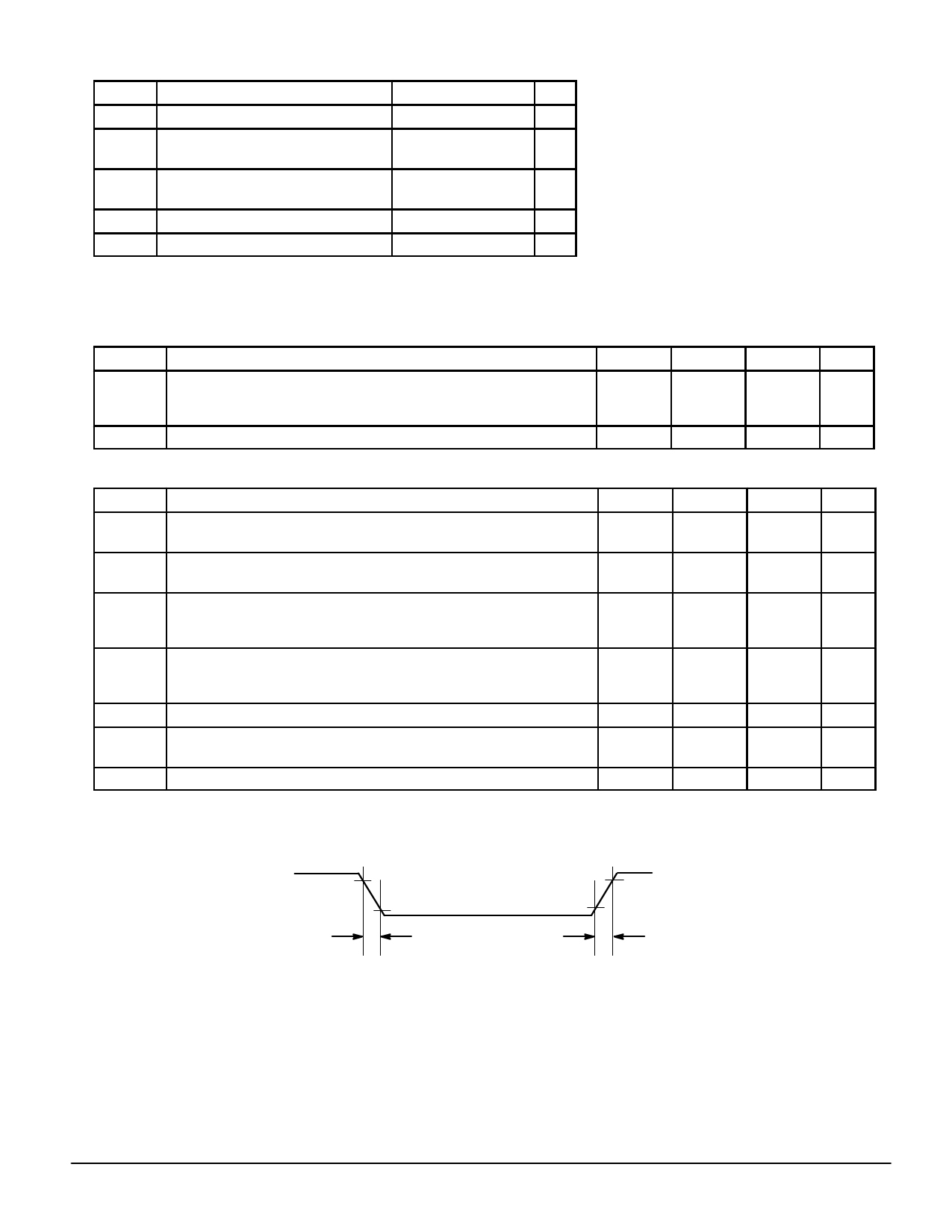
Output Signal (R, G, B, FBKG and HTONE) Cload = 30 pF, see Figure 1
tr
Rise Time
—
—
10
ns
tf
Fall Time
—
—
10
ns
FHFLB HFLB Input Frequency
—
—
100
kHz
DC CHARACTERISTICS VDD = VDD(A) = 5.0 V ± 10%, VSS = VSS(A) = 0 V, TA = 25°C, Voltage Referenced to VSS
Symbol
Characteristic
Min
Typ
Max
Unit
VOH
VOL
High Level Output Voltage
Iout = – 5 mA
Low Level Output Voltage
Iout = 5 mA
VDD – 0.8
—
—
V
—
—
VSS + 0.4
V
Digital Input Voltage (Not Including SDA and SCL)
VIL
Logic Low
VIH
Logic High
Input Voltage of Pin SDA and SCL in SPI Mode
VIL
Logic Low
VIH
Logic High
III
High–Z Leakage Current (R, G, B and FBKG)
III
Input Current (Not Including RP, VCO, R, G, B, FBKG and HTONE)
—
—
0.3 VDD
V
0.7 VDD
—
—
V
—
—
0.3 VDD
V
0.7 VDD
—
—
V
– 10
—
+ 10
µA
– 10
—
+ 10
µA
IDD
Supply Current (No Load on Any Output)
* Not a guaranteed limit.
—
9*
—
mA
90%
10%
tf
90%
10%
tr
Figure 1. Switching Characteristics
MOTOROLA
MC141540
3
Share Link: 