MC141540 View Datasheet(PDF) - Motorola => Freescale
Part Name
Description
Manufacturer
MC141540 Datasheet PDF : 12 Pages
| |||
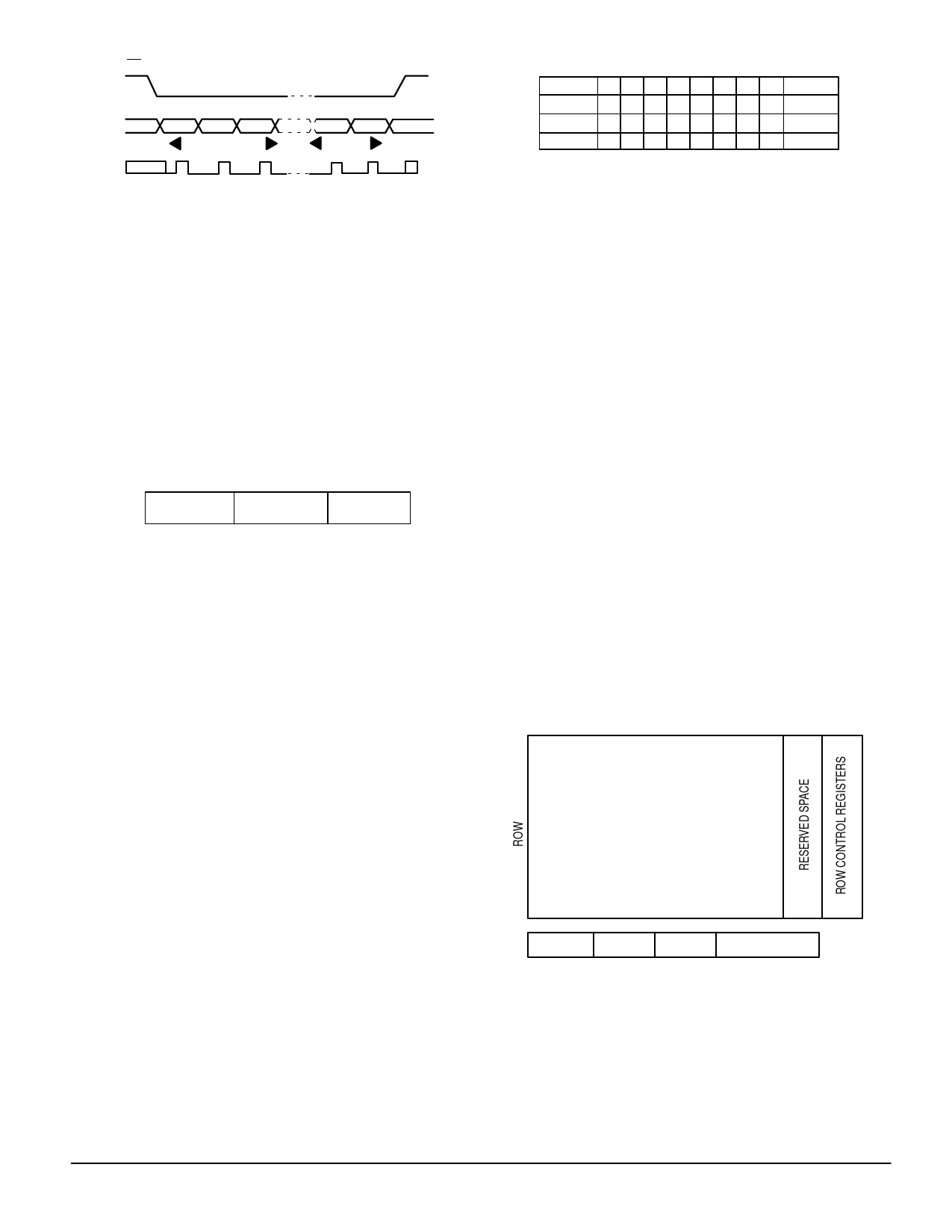
SS
MOSI
MSB
ÉÉSCKÉÉ
first byte
LSB
ÉÉÉÉ last byte
Figure 2. SPI Protocol
DATA TRANSMISSION FORMATS
After the proper identification by the receiving device, a
data train of arbitrary length is transmitted from the master.
There are three transmission formats from (a) to (c) as stated
below. The data train in each sequence consists of row ad-
dress (R), column address (C), and display information (I), as
shown in Figure 3. In format (a), display information data
must be preceded with the corresponding row address and
column address. This format is particularly suitable for updat-
ing small amounts of data between different rows. However,
if the current information byte has the same row address as
the one before, format (b) is recommended.
ÎÎroÎÎwadÎÎdr ÎÎÎÎcoÎÎladdÎÎr ÎÎÎÎinfoÎÎÎÎÎÎ
Figure 3. Data Packet
For a full–screen pattern change that requires a massive
information update, or during power–up, most of the row and
column addresses of either (a) or (b) formats will be consec-
utive. Therefore, a more efficient data transmission format (c)
should be applied. This sends the RAM starting row and col-
umn addresses once only, and then treats all subsequent
data as display information. The row and column addresses
will be automatically incremented internally for each display
information data from the starting location. Because Col-
umns 24 through 29 are unused, it is recommended that
these locations are filled with dummy data while using format
(c) to transmit.
The data transmission formats are:
(a) R – > C – > I – > R – > C – > I – > . . . . . . . . .
(b) R – > C – > I – > C – > I – > C – > I. . . . . . .
(c) R – > C – > I – > I – > I – > . . . . . . . . . . . . .
To differentiate the row and column addresses when trans-
ferring data from master, the MSB (most significant bit) is set,
as in Figure 4: ‘1’ to represent row, and ‘0’ for column ad-
dress. Furthermore, to distinguish the column address be-
tween formats (a), (b), and (c), the sixth bit of the column
address is set to ‘1’ which represents format (c), and ‘0’ for
format (a) or (b). However, there is some limitation on using
mixed formats during a single transmission. It is permissible
to change the format from (a) to (b), or from (a) to (c), or from
(b) to (a), but not from (c) back to (a) or (b).
ADDRESS
BIT
FORMAT
7 654321 0
ÎÎÎÎÎÎÎÎÎÎÎÎÎÎ ROW
1 X X X D D D D a, b, c
ÎÎÎÎÎÎÎÎÎÎÎÎÎÎ COLUMN 0 0 X D D D D D a,b
ÎÎÎÎÎÎÎÎÎÎÎÎÎÎ COLUMN 0 1 X D D D D D c
ÎÎÎÎÎÎÎÎÎÎÎÎÎÎ X: don’t care
D: valid data
Figure 4. Row & Column Address Bit Patterns
MEMORY MANAGEMENT
Internal RAM is addressed with row and column (coln)
numbers in sequence. The spaces between Row 0 and Coln
0 to Row 9 and Coln 23 are called display registers, and each
contains a character ROM address corresponding to a dis-
play location on the monitor screen. Every data row is
associated with two control registers, which are located at
Coln 30 and 31 of their respective rows, to control the char-
acter display format of that row. In addition, three window
control registers for each of the three windows, together with
three frame control registers, occupy the first 13 columns of
Row 10.
The user should handle the internal RAM address location
with care, especially those rows with double length alphanu-
meric symbols. For example, if Row n is destined to be
double height on the memory map, the data displayed on
screen Rows n and n+1 will be represented by the data con-
tained in the memory address of Row n only. The data of the
next Row n+1 on the memory map will appear on the screen
as n+2 and n+3 row space, and so on. Hence, it is not neces-
sary to load a row of blank data to compensate for the double
row. The user should minimize excessive rows of data in
memory in order to avoid overrunning the limited amount of
row space on the screen.
For rows with double width alphanumeric symbols, only
the data contained in the even numbered columns of the
memory map are shown. Odd numbered columns are
treated in the same manner as double height rows.
0
9
ÎÎÎÎÎÎÎÎÎ00 ÎÎÎÎÎÎÎÎÎÎÎÎÎÎÎÎÎÎ2 ÎÎÎÎÎÎÎÎÎ3 DÎÎÎÎÎÎÎÎÎISPLAÎÎÎÎÎÎÎÎÎ5CYO6RLEÎÎÎÎÎÎÎÎÎUGMISNTÎÎÎÎÎÎÎÎÎER8SÎÎÎÎÎÎÎÎÎ9 ÎÎÎÎÎÎÎÎÎÎÎÎÎÎÎÎÎÎ23 2ÎÎÎÎÎÎÎÎÎ4...12ÎÎÎÎÎÎÎÎÎ29 30ÎÎÎÎÎÎÎÎÎ31ÎÎÎÎÎÎÎÎÎ
10 WINDOW 1 WINDOW 2 WINDOW 3 FRAME CRTL REG
WINDOW AND FRAME CONTROL REGISTERS
Figure 5. Memory Map
MOTOROLA
MC141540
5
Share Link: 