SP503(2000) View Datasheet(PDF) - Signal Processing Technologies
Part Name
Description
Manufacturer
SP503 Datasheet PDF : 13 Pages
| |||
In DTE mode; TxD, TxC, RTS, DTR are the
drivers and RxD, RxC, CTS, DSR, DCD are the
receivers. Since there are seven drivers and
seven receivers in the SP503, the designer can
easily use the SP503 for the above signals. Other
RS-232 applications will support diagnostic func-
tions such as LL (driver), RL (driver), and TM
(receiver) which may or may not require extra
transceivers depending if other signals are not
used. Since Test Mode (TM) is a receiver for
DTE designs, the Ring Indicator (RI) receiver in
the SP503 (pin 21) can be used for TM if RI is not
used. If all the available drivers and receivers are
used in the SP503, then another RS-232 trans-
ceiver can be added. See page 230 and 231 for
suggestions on adding Sipex's RS-232 and
RS-485 transceivers.
Are the Schottky diodes used from Vcc to Vss
and from Vdd to C2- in the SP502 necessary for
the SP503?
Sipex has incorporated the Schottky diodes
(needed with the SP502) into the SP503 in order
to protect against potential start up problems due
to fast rate of rise on VCC(≥1V/µs) and overvolt-
age to the TTL inputs. However, a negative
voltage (Vin ≤ -5V) applied to the receiver inputs
while the SP503 is powered off will cause start-
up problems to the charge pump. In order to
guard against this condition, an external Schottky
diode should be placed from VCC to VDD to
minimize VCC current injection into the IC sub-
strate and allow the charge pump to operate
properly. See page 203 Figure 6 - Typical
Operating Circuit, for diode connection
schematic.
Can the SP503 be configured for V.36?
CCITT Recommendation V.36 is similar to RS-
449 where certain signals are RS-422 signals and
others are RS-423. Depending on different ap-
plications; "Transmit Data", "Terminal Timing",
"Request-to-Send", "Data Terminal Ready",
"Receive Data", "Transmit Clock", "Receive
Clock", "Clear-to-Send", "Data Carrier Detect",
and "DataSet Ready" are specified as Category 1
Circuits where the protocol is RS-422 for rates
over 20kbps. All other circuits are Category 2
Circuits which are specified as RS-423 circuits.
Depending on particular signals, the SP503 can
be easily used for V.36.
When the two drivers, ST and TT, are in tri-state
mode, what will the driver outputs tolerate for
maximum short circuit voltages? And the re-
ceiver, SCT, input?
The driver outputs will tolerate up to ±16.0V
without any damage to the circuit regardless of
whether or not ST and TT are in tri-state mode.
The tri-state circuitry does not affect the short
circuit protection on the driver outputs. The SCT
receiver input will tolerate up to ±16.0V without
any damage to the input structure regardless of
whether or not SCT is in tri-state mode.
What does Sipex recommend for transient volt-
age suppression techniques for the SP503?
For our evaluation boards, Sipex uses transient
voltage suppressor ICs from ProTek Devices,
model numbers LCA05C to LCA15C. The two
digits in the part number pertain to the rated
stand-off voltage, VWM, which is the maximum
working DC voltage applied to the device. These
TVS devices are especially designed for serial
data communications because of their low ca-
pacitance and low impedance. However, please
be aware that VWM values below the specified
input range of the transceiver will affect the input
impedance. For example, it would be fine to use
a 5V V value for RS-422 but for RS-232, the
WM
receiver input voltage range is ±15V where lower
VWM voltages will drive the impedance to ground.
Another recommended manufacturer is AVX
Corporation TransGuard series of TVS compo-
nents. AVX offers a variety of surface mount
back-to-back diodes.
ProTek Devices • P.O. Box 3129 • Tempe, AZ. 85280
• 602-431-8101
AVX Corporation • Myrtle Beach, SC • 803-448-9411
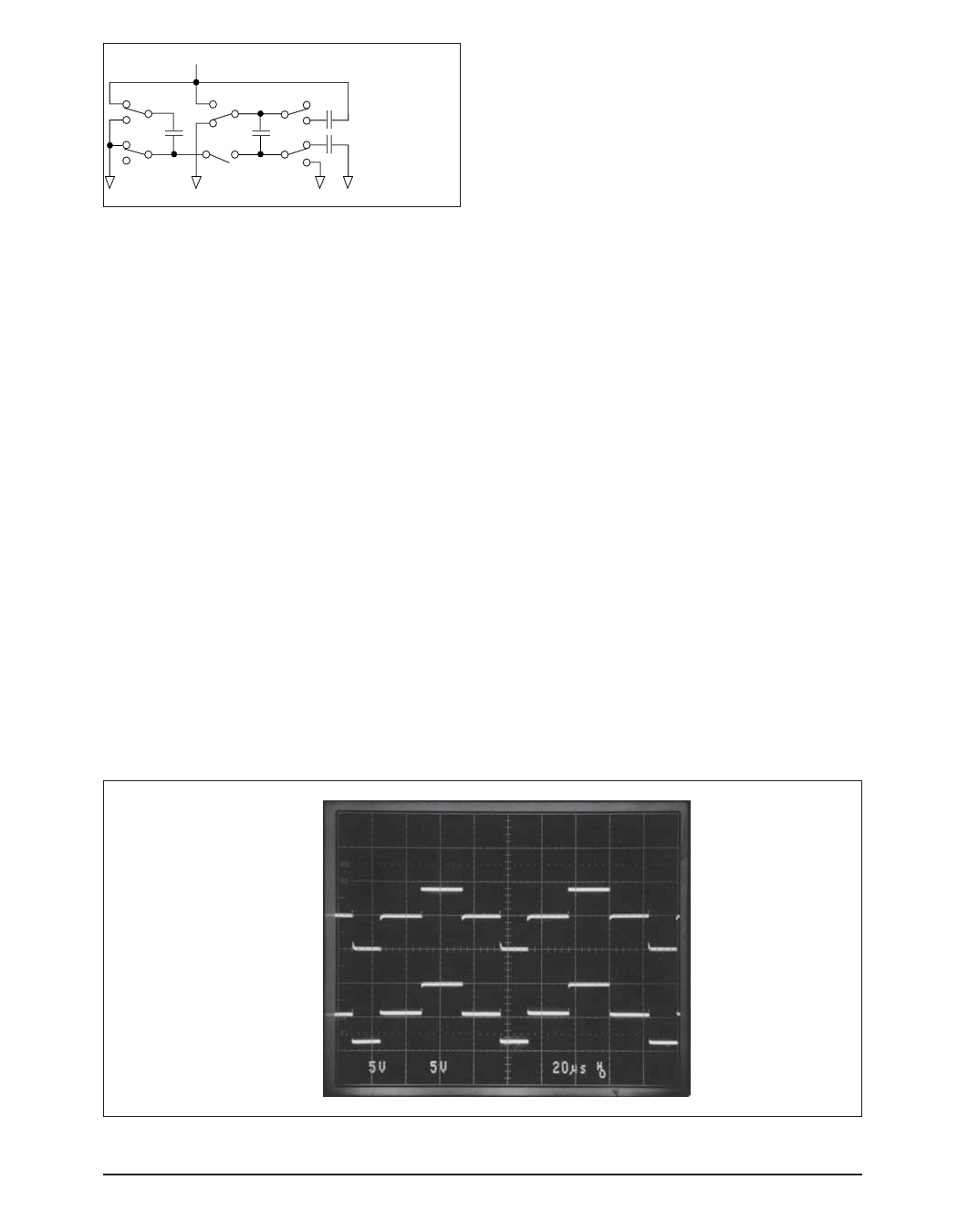
The drawing on page 232 shows the SP503
configured with the ProTek SM16LC15C TVS
devices to protect the drivers and receivers from
ESD and over-voltage.
Will the SP503 conform to the physical layer
testing specified by NET1/NET2 for X.21 and
X.25 systems?
Sipex initiated a component level test for NET1/
NET2 for V.28, V.10, V.11, V.35 protocols. The
SP503 passed all the physical layer testing re-
quirements prescribed by NET1/NET2. A full
test report can be furnished upon request.
SP503AN
SP503 Application Note
9
© Copyright 2000 Sipex Corporation
Share Link: 