M2716F1 View Datasheet(PDF) - STMicroelectronics
Part Name
Description
Manufacturer
M2716F1 Datasheet PDF : 9 Pages
| |||
M2716
Table 2. Absolute Maximum Ratings
Symbol
Parameter
Value
Unit
TA
Ambient Operating Temperature
grade 1
grade 6
0 to 70
–40 to 85
°C
TBIAS
Temperature Under Bias
grade 1
grade 6
–10 to 80
–50 to 95
°C
TSTG
Storage Temperature
–65 to 125
°C
VCC
Supply Voltage
–0.3 to 6
V
VIO
Input or Output Voltages
–0.3 to 6
V
VPP
Program Supply
–0.3 to 26.5
V
PD
Power Dissipation
1.5
W
Note: Except for the rating "Operating Temperature Range", stresses above those listed in the Table "Absolute Maximum Ratings" may cause
permanent damage to the device. These are stress ratings only and operation of the device at these or any other conditions above those
indicated in the Operating sections of this specification is not implied. Exposure to Absolute Maximum Rating conditions for extended periods
may affect device reliability. Refer also to the SGS-THOMSON SURE Program and other relevant quality documents.
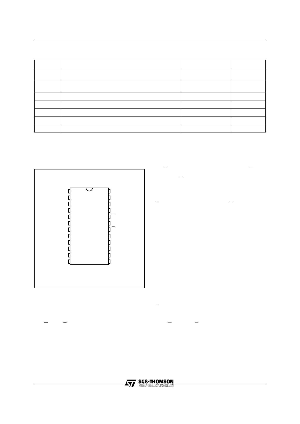
Figure 2. DIP Pin Connections
A7 1
A6 2
A5 3
A4 4
A3 5
A2 6
A1 7
A0 8
Q0 9
Q1 10
Q2 11
VSS 12
M2716
24 VCC
23 A8
22 A9
21 VPP
20 G
19 A10
18 EP
17 Q7
16 Q6
15 Q5
14 Q4
13 Q3
AI00785
DEVICE OPERATION
The M2716 has 3 modes of operation in the normal
system environment. These are shown in Table 3.
Read Mode. The M2716 read operation requires
that G = VIL, EP = VIL and that addresses A0-A10
have been stabilized. Valid data will appear on the
output pins after time tAVQV, tGLQV or tELQV (see
Switching Time Waveforms) depending on which is
limiting.
Deselect Mode. The M2716 is deselected by mak-
ing G = VIH. This mode is independent of EP and
the condition of the addresses. The outputs are
Hi-Z when G = VIH. This allows tied-OR of 2 or more
M2716’s for memory expansion.
Standby Mode (Power Down). The M2716 may
be powered down to the standby mode by making
EP = VIH. This is independent of G and automat-
ically puts the outputs in the Hi-Z state. The power
is reduced to 25% (132 mW max) of the normal
operating power. VCC and VPP must be maintained
at 5V. Access time at power up remains either tAVQV
or tELQV (see Switching Time Waveforms).
Programming
The M2716 is shipped from SGS-THOMSON com-
pletely erased. All bits will be at “1" level (output
high) in this initial state and after any full erasure.
Table 3 shows the 3 programming modes.
Program Mode. The M2716 is programmed by
introducing “0"s into the desired locations. This is
done 8 bits (a byte) at a time. Any individual address,
sequential addresses, or addresses chosen at ran-
dom may be programmed. Any or all of the 8 bits
associated with an address location may be pro-
grammed with a single program pulse applied to the
EP pin. All input voltage levels including the program
pulse on chip enable are TTL compatible.
The programming sequence is: with VPP = 25V, VCC
= 5V, G = VIH and EP = VIL, an address is selected
and the desired data word is applied to the output
pins (VIL = “0" and VIH = ”1" for both address and
data). After the address and data signals are stable
the program pin is pulsed from VIL to VIH with a
2/9
Share Link: 