M27V400 View Datasheet(PDF) - STMicroelectronics
Part Name
Description
Manufacturer
M27V400 Datasheet PDF : 14 Pages
| |||
M27V400
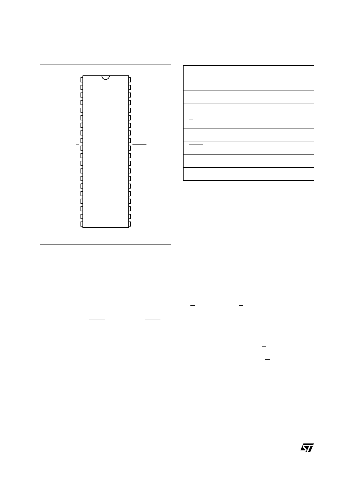
Figure 2. DIP Connections
A17
A7
A6
A5
A4
A3
A2
A1
A0
E
VSS
G
Q0
Q8
Q1
Q9
Q2
Q10
Q3
Q11
1
40 A8
2
39 A9
3
38 A10
4
37 A11
5
36 A12
6
35 A13
7
34 A14
8
33 A15
9
32 A16
10
31
M27C400
BYTEVPP
11
30 VSS
12
29 Q15A–1
13
28 Q7
14
27 Q14
15
26 Q6
16
25 Q13
17
24 Q5
18
23 Q12
19
22 Q4
20
21 VCC
AI01635
DEVICE OPERATION
The operating modes of the M27V400 are listed in
the Operating Modes Table. A single power supply
is required in the read mode. All inputs are TTL
compatible except for VPP and 12V on A9 for the
Electronic Signature.
Read Mode
The M27V400 has two organisations, Word-wide
and Byte-wide. The organisation is selected by the
signal level on the BYTEVPP pin. When BYTEVPP
is at VIH the Word-wide organisation is selected
and the Q15A–1 pin is used for Q15 Data Output.
When the BYTEVPP pin is at VIL the Byte-wide or-
ganisation is selected and the Q15A–1 pin is used
for the Address Input A–1. When the memory is
Table 1. Signal Names
A0-A17
Address Inputs
Q0-Q7
Data Outputs
Q8-Q14
Data Outputs
Q15A–1
Data Output / Address Input
E
Chip Enable
G
Output Enable
BYTEVPP
Byte Mode / Program Supply
VCC
Supply Voltage
VSS
Ground
logically regarded as 16 bit wide, but read in the
Byte-wide organisation, then with A–1 at VIL the
lower 8 bits of the 16 bit data are selected and with
A–1 at VIH the upper 8 bits of the 16 bit data are
selected.
The M27V400 has two control functions, both of
which must be logically active in order to obtain
data at the outputs. In addition the Word-wide or
Byte- wide organisation must be selected.
Chip Enable (E) is the power control and should be
used for device selection. Output Enable (G) is the
output control and should be used to gate data to
the output pins independent of device selection.
Assuming that the addresses are stable, the ad-
dress access time (tAVQV) is equal to the delay
from E to output (tELQV). Data is available at the
output after a delay of tGLQV from the falling edge
of G, assuming that E has been low and the ad-
dresses have been stable for at least tAVQV-tGLQV.
Standby Mode
The M27V400 has a standby mode which reduces
the supply current from 30mA to 20µA. The
M27V400 is placed in the standby mode by apply-
ing a CMOS high signal to the E input. When in the
standby mode, the outputs are in a high imped-
ance state, independent of the G input.
2/14
Share Link: 