2SB808 Просмотр технического описания (PDF) - SANYO -> Panasonic
Номер в каталоге
Компоненты Описание
производитель
2SB808 Datasheet PDF : 6 Pages
| |||
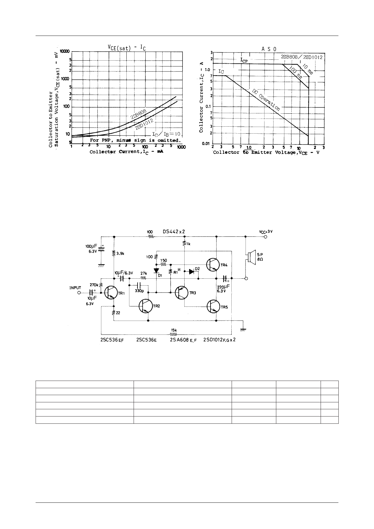
2SB808/2SD1012
Sample Application Circuit : Low-voltage 3V (PO 120mW) ITL-OTL power amplifier.
· Circuit configuration
For obtaining an output of more than 100mW, the middle-point voltage at the output stage and the collector voltage
of the driver transistor must be VCC/2. Therefore, the output stage is of quasi complementary configuration com-
posed of npn/npn transistors. The phase is reversed by the 2SA608 and the middle-point voltage are the output
stage and the collector voltage of the driver transistor are more to be VCC/2 so that the output can be maximized.
Unit (resistance : Ω, capacitance : F)
R1 : Used control idle current
For R1=820Ω, use rank F for [TR4, 5 (2SD1012)].
For R1=680Ω, use rank G for [TR4, 5 (2SD1012)].
Main Specifications
Characteristic
Current dissipation
Output power
Votlage gain
Total harmonic distortion
Input resistance
Note : for above-mentioned hFE rank.
Conditions
Quiescent, total current dissipation
THD=10%
PO=10mW
PO=50mW
PO=10mW
f=400Hz
f=1kHz
Unit
11.0 to 15.5
11.0 to 15.5
mA
120 to 125
127 to 130
mW
43.3 to 45.5
43.5 to 45.7
dB
1.4 to 2.6
1.3 to 2.5
%
10.4 to 20.5
11.0 to 21.0
kΩ
No.676–3/5
Share Link: 