T405Q-600B(2002) Просмотр технического описания (PDF) - STMicroelectronics
Номер в каталоге
Компоненты Описание
производитель
T405Q-600B Datasheet PDF : 7 Pages
| |||
T405Q-600B-TR & T405Q-600H
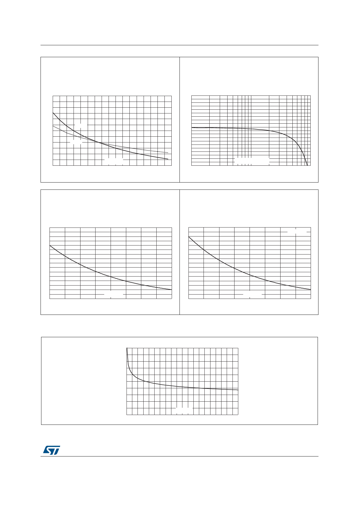
Fig. 7: Relative variation of gate trigger current,
holding current and latching current versus junc-
tion temperature (typical values).
Fig. 8: Relative variation of critical rate of decrease
of main current versus reapplied dV/dt (typical val-
ues).
IGT, IH, IL[Tj] / IGT, IH, IL [Tj = 25°C]
3.0
(dI/dt)c [(dV/dt)c] / Specified (dI/dt)c
2.0
1.8
2.5
1.6
1.4
2.0
IGT
1.2
1.5
1.0
0.8
1.0
IH & IL
0.6
0.5
Tj(°C)
0.0
-40 -30 -20 -10 0 10 20 30 40 50 60 70 80 90 100 110 120 130
0.4
0.2
0.0
0.1
(dV/dt)c (V/µs)
1.0
10.0
Fig. 9: Relative variation of critical rate of decrease
of main current versus junction temperature.
Fig. 10: Relative variation of static dV/dt immunity
versus junction temperature.
(dI/dt)c [Tj] / (dI/dt)c [Tj = 125°C]
8
7
6
5
4
3
2
1
Tj(°C)
0
25
50
75
100
dV/dt [Tj] / dV/dt [Tj = 125°C]
8
7
6
5
4
3
2
1
0
125
25
Tj(°C)
50
75
VD=VR=400V
100
125
Fig. 11: Thermal resistance junction to ambient
versus copper surface under tab (epoxy printed
circuit board FR4, Cu = 35µm).
Rth(j-a)(°C/W)
100
90
80
70
60
50
40
30
20
10
S(cm²)
0
0
2
4
6
8
10 12 14 16 18 20
5/7
Share Link: 