1CZ41H Просмотр технического описания (PDF) - Sharp Electronics
Номер в каталоге
Компоненты Описание
производитель
1CZ41H Datasheet PDF : 5 Pages
| |||
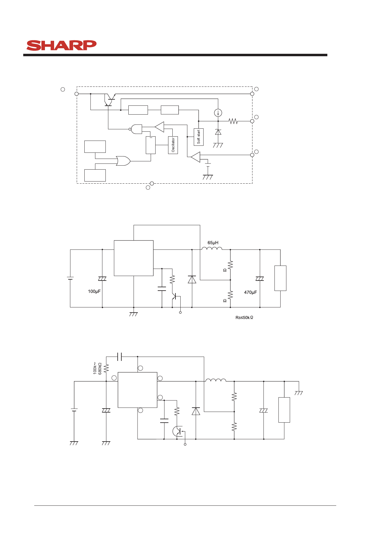
Fig.15 Block Diagram
1 VIN
Overcurrent
detection
circuit
Voltage
regulator
ON/OFF
circuit
PWM COMP.
_
+
Q
F/F R
S
Overheat
detection
circuit
3 COM
Fig.16 Step Down Type Circuit Diagram
_ ERROR AMP.
+
Vref
PQ1CZ41H2ZxH
2 VOUT
5 ON/OFF control
4 Oadj
VIN
8 to 35V
④
①
②
PQ1CZ41H2ZxH
⑤
+
CIN
③
CS
RS
L
R2
3k
D
R1
1k
ON/OFF control signal
Fig.17 Polarity Inversion Type Circuit Diagram
0.47~1μF
VO 5V
+
CO
Load
VIN
5~30V
4
1
2
PQ1CZ41H2ZxH
5
+
CIN
100μF
3
CS
L
65μH
RS
D
R2
3kΩ
+
CO
2200μF
R1
1kΩ
Load
ON/OFF control signal
RS≦50kΩ
VO -5V
In case that polarity is reverse, depending on the conditions,there is cases that output voltage can not gain,
please use this device after confirming the output voltage at the actual conditions.
Sheet No.: OP06041
5
Share Link: 