IRFRC20(2013) Просмотр технического описания (PDF) - Vishay Semiconductors
Номер в каталоге
Компоненты Описание
производитель
IRFRC20 Datasheet PDF : 12 Pages
| |||
www.vishay.com
IRFRC20, IRFUC20, SiHFRC20, SiHFUC20
Vishay Siliconix
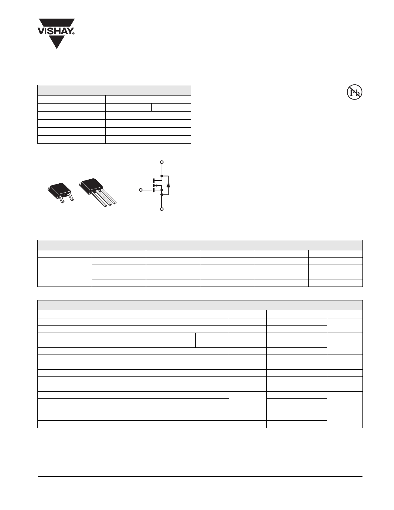
Power MOSFET
PRODUCT SUMMARY
VDS (V)
RDS(on) ()
Qg (Max.) (nC)
Qgs (nC)
Qgd (nC)
Configuration
600
VGS = 10 V
4.4
18
3.0
8.9
Single
D
DPAK
(TO-252)
IPAK
(TO-251)
D
D
G
GS
GD S
S
N-Channel MOSFET
FEATURES
• Dynamic dV/dt Rating
• Repetitive Avalanche Rated
• Surface Mount (IRFRC20, SiHFRC20)
• Straight Lead (IRFUC20, SiHFUC20)
• Available in Tape and Reel
• Fast Switching
• Ease of Paralleling
• Material categorization: For definitions of compliance
please see www.vishay.com/doc?99912
DESCRIPTION
Third generation power MOSFETs from Vishay provide the
designer with the best combination of fast switching,
ruggedized device design, low on-resistance and
cost-effectiveness.
The DPAK is designed for surface mounting using vapor
phase, infrared, or wave soldering techniques. The straight
lead version (IRFUC, SiHFUC series) is for through-hole
mounting applications. Power dissipation levels up to 1.5 W
are possible in typical surface mount applications.
ORDERING INFORMATION
Package
DPAK (TO-252)
Lead (Pb)-free and
Halogen-free
SiHFRC20-GE3
Lead (Pb)-free
IRFRC20PbF
SiHFRC20-E3
Note
a. See device orientation.
DPAK (TO-252)
SiHFRC20TRL-GE3
IRFRC20TRLPbFa
SiHFRC20TL-E3a
DPAK (TO-252)
SiHFRC20TR-GE3
IRFRC20TRPbFa
SiHFRC20T-E3a
DPAK (TO-252)
SiHFRC20TRR-GE3
IRFRC20TRRPbFa
SiHFRC20TR-E3a
IPAK (TO-251)
SiHFUC20-GE3
IRFUC20PbF
SiHFUC20-E3
ABSOLUTE MAXIMUM RATINGS (TC = 25 °C, unless otherwise noted)
PARAMETER
SYMBOL
Drain-Source Voltage
Gate-Source Voltage
Continuous Drain Current
Pulsed Drain Currenta
Linear Derating Factor
VDS
VGS
VGS at 10 V
TC = 25 °C
TC = 100 °C
ID
IDM
Linear Derating Factor (PCB Mount)e
Single Pulse Avalanche Energyb
Repetitive Avalanche Currenta
Repetitive Avalanche Energya
Maximum Power Dissipation
Maximum Power Dissipation (PCB Mount)e
Peak Diode Recovery dV/dtc
TC = 25 °C
TA = 25 °C
EAS
IAR
EAR
PD
dV/dt
Operating Junction and Storage Temperature Range
TJ, Tstg
Soldering Recommendations (Peak Temperature)d
for 10 s
Notes
a. Repetitive rating; pulse width limited by maximum junction temperature (see fig. 11).
b. VDD = 50 V, starting TJ = 25 °C, L = 37 mH, Rg = 25 , IAS = 2.0 A (see fig. 12).
c. ISD 2.0 A, dI/dt 40 A/μs, VDD VDS, TJ 150 °C.
d. 1.6 mm from case.
e. When mounted on 1" square PCB (FR-4 or G-10 material).
LIMIT
600
± 20
2.0
1.3
8.0
0.33
0.020
74
2.0
4.2
42
2.5
3.0
- 55 to + 150
260
UNIT
V
A
W/°C
mJ
A
mJ
W
V/ns
°C
S13-0166-Rev. E, 04-Feb-13
1
Document Number: 91285
For technical questions, contact: hvm@vishay.com
THIS DOCUMENT IS SUBJECT TO CHANGE WITHOUT NOTICE. THE PRODUCTS DESCRIBED HEREIN AND THIS DOCUMENT
ARE SUBJECT TO SPECIFIC DISCLAIMERS, SET FORTH AT www.vishay.com/doc?91000
Share Link: 