MAX1967 Просмотр технического описания (PDF) - Maxim Integrated
Номер в каталоге
Компоненты Описание
производитель
MAX1967 Datasheet PDF : 15 Pages
| |||
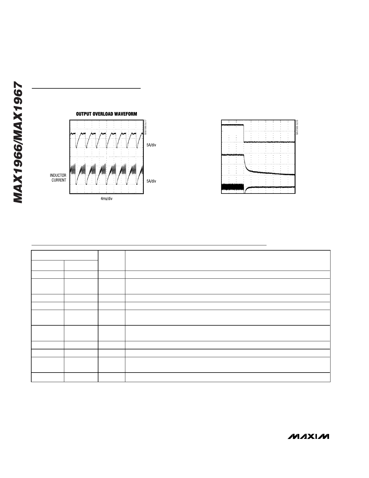
Low-Cost Voltage-Mode PWM
Step-Down Controllers
(TA = +25°C, unless otherwise noted.)
Typical Operating Characteristics (continued)
IOUT
VIN = 5.0V
VIN = 1.8V
L = 22µF
SHUTDOWN WAVEFORMS
NO LOAD
VIN
2V/div
VOUT
INDUCTOR
CURRENT
10ms/div
1V/div
1A/div
Pin Description
PIN
MAX1966
1
MAX1967
10
2
1
3
2
—
3
4
4
—
5
5
6
6
7
7
8
8
9
NAME
BST
COMP/EN
FB
VCC
VIN
VL
DL
GND
LX
DH
FUNCTION
Positive Supply of DH Driver. Connect 0.1µF ceramic capacitor between BST and LX.
Compensation Pin. Pulling COMP/EN low with an open-collector or open-drain device
turns off the output.
Feedback Input. Connect a resistive divider network to set VOUT. FB threshold is 0.8V.
Internal Chip Supply. Connect to VL via a 10Ω resistor.
Power Supply for LDO Regulator in the MAX1967 and Chip Supply for the MAX1966.
Bypass with a ceramic capacitor to ground (see application circuit).
Output of Internal 5V LDO. Bypass with a 2.2µF capacitor to GND, or if VIN < 5.5,
connect VL to VIN and bypass with a 0.1µF capacitor to GND.
Low-Side External MOSFET Gate-Driver Output. DL swings from VL to GND.
Ground and Negative Current-Sense Input
Inductor Switching Node. LX is used for both current limit and the return supply of the
DH driver.
High-Side External MOSFET Gate-Driver Output. DH swings from BST to LX.
6 _______________________________________________________________________________________
Share Link: 