MAX500 Просмотр технического описания (PDF) - Maxim Integrated
Номер в каталоге
Компоненты Описание
производитель
MAX500 Datasheet PDF : 12 Pages
| |||
CMOS, Quad, Serial-Interface
8-Bit DAC
____________________________Typical Operating Characteristics (continued)
OUTPUT SINK CURRENT
vs. OUTPUT VOLTAGE
16
VSS = -5V
14
12
RO ≅ 200Ω
10
VSS = 0V
8
6
4
2
0
0
2
4
6
8
10
VOUT (V)
12
10
8
6
4
2
0
-2
-4
-6
-55
SUPPLY CURRENT
vs. TEMPERATURE
IDD
ISS
-25 0 25 50 75 100 125
TEMPERATURE (°C)
ZERO-CODE ERROR
vs. TEMPERATURE
2.0
1.5
VOUTA
1.0
0.5
VOUTB
0.0
VOUTC
-0.5
-1.0
VOUTD
-1.5
VSS = -5V
-2.0
-55 -25 0 25 50 75
TEMPERATURE (°C)
100 125
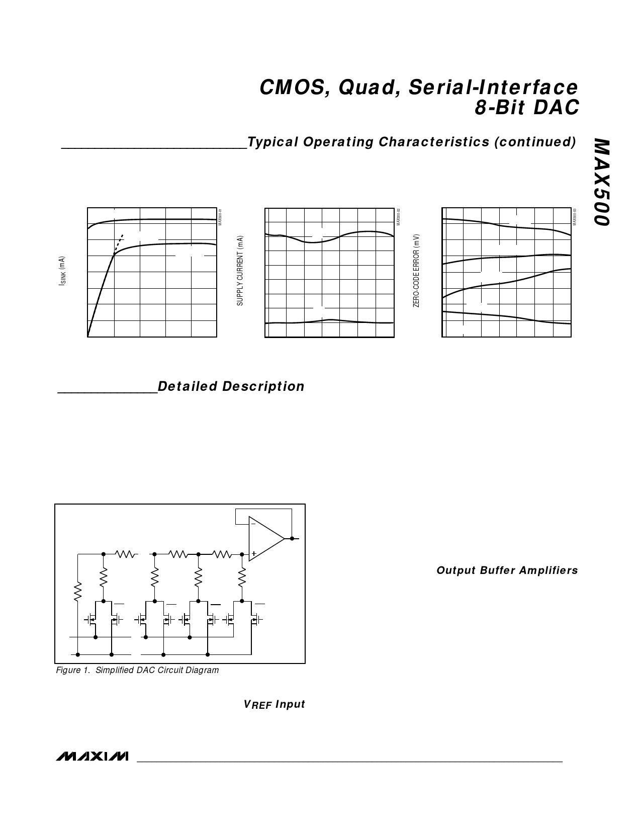
_______________Detailed Description
The MAX500 has four matched voltage-output digital-to-
analog converters (DACs). The DACs are “inverted”
R-2R ladder networks which convert 8 digital bits into
equivalent analog output voltages in proportion to the
applied reference voltage(s). Two DACs in the MAX500
have a separate reference input while the other two
DACs share one reference input. A simplified circuit
diagram of one of the four DACs is provided in Figure 1.
R
R
R
VOUT
…
2R
2R
2R
2R
2R
DB0
DB5
DB6
DB7
VREF DB0
DB5
…
DB6
DB7
AGND
…
Figure 1. Simplified DAC Circuit Diagram
VREF Input
The voltage at the VREF pins (pins 4, 12, and 13) sets
the full-scale output of the DAC. The input impedance
of the VREF inputs is code dependent. The lowest
value, approximately 11kΩ (5.5kΩ for VREFA/B), occurs
when the input code is 01010101. The maximum value
of infinity occurs when the input code is 00000000.
Because the input resistance at VREF is code depen-
dent, the DAC’s reference sources should have an out-
put impedance of no more than 20Ω (no more than
10Ω for VREFA/B). The input capacitance at VREF is
also code dependent and typically varies from 15pF to
35pF (30pF to 70pF for VREFA/B). VOUTA, VOUTB,
VOUTC, and VOUTD can be represented by a digitally
programmable voltage source as:
VOUT = Nb x VREF / 256
where Nb is the numeric value of the DAC’s binary
input code.
Output Buffer Amplifiers
All voltage outputs are internally buffered by precision
unity-gain followers, which slew at greater than 3V/µs.
When driving 2kΩ in parallel with 100pF with a full-scale
transition (0V to +10V or +10V to 0V), the output settles
to ±1/2LSB in less than 4µs. The buffers will also drive
2kΩ in parallel with 500pF to 10V levels without oscilla-
tion. Typical dynamic response and settling perfor-
mance of the MAX500 is shown in Figures 2 and 3.
A simplified circuit diagram of an output buffer is
shown in Figure 4. Input common-mode range to
AGND is provided by a PMOS input structure. The out-
put circuitry incorporates a pull-down circuit to actively
drive VOUT to within +15mV of the negative supply
(VSS). The buffer circuitry allows each DAC output to
_______________________________________________________________________________________ 5
Share Link: 