MAX3051 Просмотр технического описания (PDF) - Maxim Integrated
Номер в каталоге
Компоненты Описание
производитель
MAX3051 Datasheet PDF : 13 Pages
| |||
MAX3051
+3.3V, 1Mbps, Low-Supply-Current
CAN Transceiver
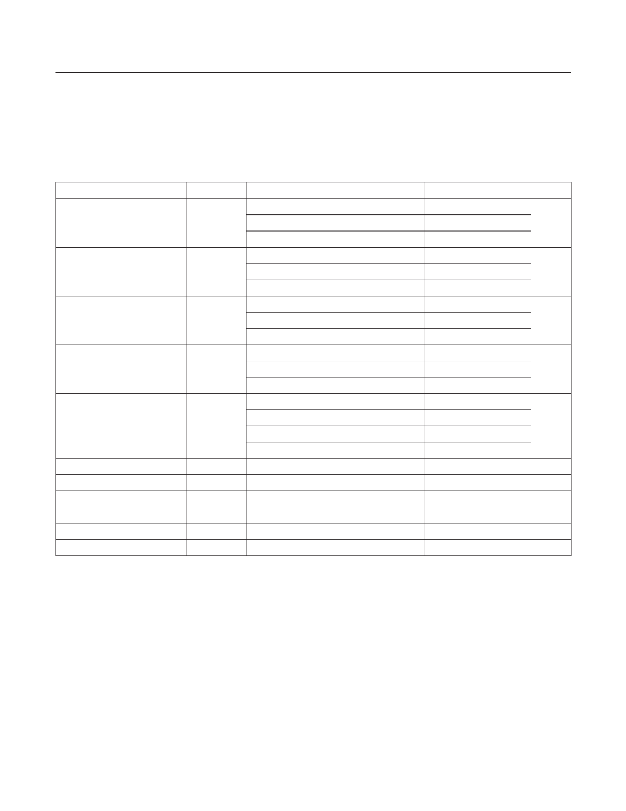
Timing Characteristics
(VCC = +3.3V ±5%, RL = 60Ω, CL = 100pF, TA = TMIN to TMAX, unless otherwise noted. Typical values are at VCC = +3.3V and
TA = +25°C.)
PARAMETER
Delay TXD to Bus Active
(Figure 1)
Delay TXD to Bus Inactive
(Figure 1)
Delay Bus to Receiver Active
(Figure 1)
Delay Bus to Receiver Inactive
(Figure 1)
Differential-Output Slew Rate
Bus Dominant to RXD Active
Standby to Receiver Active
SHDN to Bus Inactive
SHDN to Receiver Active
SHDN to Standby
ESD Protection
SYMBOL
tONTXD
tOFFTXD
tONRXD
tOFFRXD
SR
tDRXDL
tSBRXDL
tOFFSHDN
tONSHDN
tSHDNSB
CONDITIONS
VRS = 0V (≤ 1Mbps)
RRS = 25kΩ (≤ 500kbps)
RRS = 100kΩ (≤ 125kbps)
VRS = 0V (≤ 1Mbps)
RRS = 25kΩ (≤ 500kbps)
RRS = 100kΩ (≤ 125kbps)
VRS = 0V (≤ 1Mbps)
RRS = 25kΩ (≤ 500kbps)
RRS = 100kΩ (≤ 125kbps)
VRS = 0V (≤ 1Mbps)
RRS = 25kΩ (≤ 500kbps)
RRS = 100kΩ (≤ 125kbps)
VRS = 0V (≤ 1Mbps)
RRS = 25kΩ (≤ 500kbps)
RRSS = 100kΩ (≤ 125kbps)
RRS = 200kΩ (≤ 62.5kbps)
VRS > 0.8 x VCC, standby, Figure 2
BUS dominant, Figure 2
TXD = GND, Figure 3 (Note 2)
BUS dominant, Fi gur e 3 (Note 3)
Figure 4
Human Body Model
MIN TYP MAX UNITS
50
183
ns
770
70
226
ns
834
80
200
ns
730
100
245
ns
800
96
12.5
V/μs
2.9
1.6
1
μs
4
μs
1
μs
4
μs
20
μs
±12
kV
Note 1: All currents into device are positive; all currents out of the device are negative. All voltages are referenced to device
ground, unless otherwise noted.
Note 2: No other devices on the BUS.
Note 3: BUS externally driven.
www.maximintegrated.com
Maxim Integrated │ 4
Share Link: 