EVAL-AD5425EB Просмотр технического описания (PDF) - Analog Devices
Номер в каталоге
Компоненты Описание
производитель
EVAL-AD5425EB Datasheet PDF : 28 Pages
| |||
AD5425
SPECIFICATIONS
VDD = 2.5 V to 5.5 V, VREF = 10 V, IOUT2 = 0 V. Temperature range for Y version: −40°C to +125°C. All specifications TMIN to TMAX, unless
otherwise noted. DC performance measured with OP177, ac performance with AD8038, unless otherwise noted.
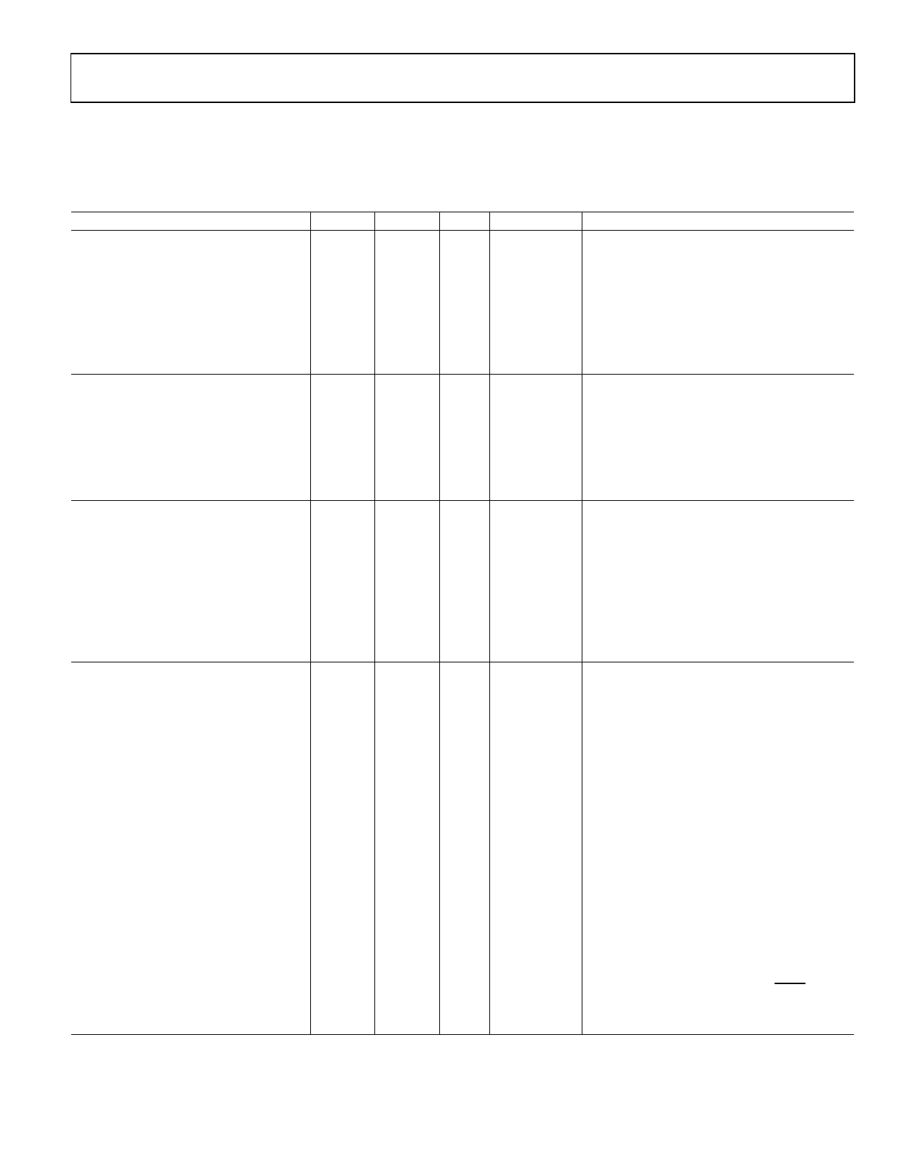
Table 1.
Parameter
STATIC PERFORMANCE
Resolution
Relative Accuracy
Differential Nonlinearity
Gain Error
Gain Error Temperature Coefficient
Output Leakage Current
REFERENCE INPUT1
Reference Input Range
VREF Input Resistance
RFB Resistance
Input Capacitance
Code Zero Scale
Code Full Scale
DIGITAL INPUT/OUTPUT1
Input High Voltage, VIH
Input Low Voltage, VIL
Output High Voltage, VOH
Output Low Voltage, VOL
Input Leakage Current, IIL
Input Capacitance
DYNAMIC PERFORMANCE1
Reference Multiplying Bandwidth
Output Voltage Settling Time
Measured to ±1 mV
Measured to ±4 mV
Measured to ±16 mV
Digital Delay
10% to 90% Settling Time
Digital-to-Analog Glitch Impulse
Multiplying Feedthrough Error
Output Capacitance
IOUT1
IOUT2
Digital Feedthrough
Analog THD
Min
Typ
±5
±10
8
10
8
10
3
5
1.7
VDD − 1
VDD − 0.5
4
10
90
55
50
40
15
2
70
48
12
25
22
10
0.1
81
Max Unit
Conditions/Comments
8
±0.25
±0.5
±10
±10
±20
Bits
LSB
LSB
mV
ppm FSR/°C
nA
nA
Guaranteed monotonic
Data = 0x0000, TA = 25°C, IOUT1
Data = 0x0000, T = −40°C to +125°C, IOUT 1
V
12
kΩ
12
kΩ
Input resistance TC = −50 ppm/°C
Input resistance TC = −50 ppm/°C
6
pF
8
pF
V
0.6 V
V
V
0.4 V
0.4 V
1
μA
10
pF
VDD = 4.5 V to 5 V, ISOURCE = 200 μA
VDD = 2.5 V to 3.6 V, ISOURCE = 200 μA
VDD = 4.5 V to 5 V, ISINK = 200 μA
VDD = 2.5 V to 3.6 V, ISINK = 200 μA
MHz
160 ns
110 ns
100 ns
75
ns
30
ns
nV-s
dB
dB
VREF = ±3.5 V, DAC loaded all 1s
VREF = ±3.5 V, RLOAD = 100 Ω, DAC latch
alternately loaded with 0s and 1s
Interface delay time
Rise and fall time, VREF = 10 V, RLOAD = 100 Ω
1 LSB change around major carry VREF = 0 V
DAC latch loaded with all 0s. VREF = ±3.5 V
1 MHz
10 MHz
17
pF
30
pF
25
pF
12
pF
nV-s
dB
All 0s loaded
All 1s loaded
All 0s loaded
All 1s loaded
Feedthrough to DAC output with SYNC high
and alternate loading of all 0s and all 1s
VREF = 3.5 V p-p; all 1s loaded, f = 1 kHz
Rev. A | Page 3 of 28
Share Link: 