AD6654 Просмотр технического описания (PDF) - Analog Devices
Номер в каталоге
Компоненты Описание
производитель
AD6654 Datasheet PDF : 88 Pages
| |||
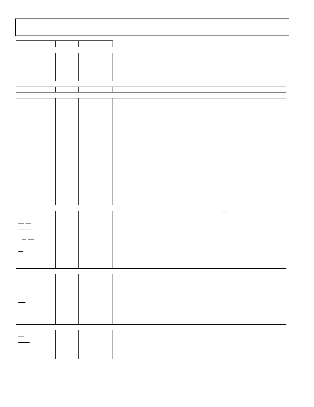
AD6654
Name
Type
DDC INPUTS
CLK
Input
SYNC0
Input
SYNC1
Input
SYNC2
Input
SYNC3
Input
DDC OUTPUTS
EXPC [2:0]
Output
DDC OUTPUT PORTS
PCLK
Bi-dir
PADATA[15:0]
Output
PACH[2:0]
Output
PAIQ
Output
PAGAIN
Output
PAACK
Input
PAREQ
Output
PBDATA[15:0]
Output
PBCH[2:0]
Output
PBIQ
Output
PBGAIN
Output
PBACK
Input
PBREQ
Output
PCDATA[15:0]
Output
PCCH[2:0]
Output
PCIQ
Output
PCGAIN
Output
PCACK
Input
PCREQ
Output
MICROPORT CONTROL
D[15:0]
Bi-Dir
A[7:0]
Input
DS (RD)
Input
DTACK (RDY)1
Output
Pin Number
A11
T10
R11
P11
T11
D11, C11, B11
T4
See Table 12
D8, R5, C8
A8
A9
B8
N6
See Table 12
P10, P8, R8
T7
R10
P9
N8
See Table 12
M5, A6, R1
P1
R2
E5
P2
See Table 12
See Table 12
B4
C3
R/W (WR)
Input
MODE
Input
CS
Input
CPUCLK
Input
CHIPID[3:0]
Input
SERIAL PORT CONTROL
SCLK
SDO1
Input
Output
SDI2
Input
STFS
Input
SRFS
Input
SCS
Input
MSB_FIRST
Input
C4
C2
D3
A4
C1, E1, B3, B2
A4
C3
K3
C4
B4
D3
D2
SMODE
MISC PINS
DNC
IRP1
RESET
EXT_FILTER
Input
-------
Output
Input
Input
F1
B12, T9
E2
F4
D1
1 Pins with internal pull-up resistor of nominal 70 kΩ.
2 Pins with internal pull-down resistor of nominal 70 kΩ.
Function
DDC Clock Input.
Synchronization Input 0. SYNC pins are independent of channels.
Synchronization Input 1.
Synchronization Input 2.
Synchronization Input 3.
External VGA Gain Control Bits. GND all pins if not used.
Parallel Output Port Clock. PCLK is bi-directional: master mode = output, slave mode = input.
Parallel Output Port A Data Bus.
Channel Indicator Output Port A.
Parallel Port A I/Q Data Indicator. Logic 1 indicates I data on data bus.
Parallel Port A Gain Word Output Indicator. Logic 1 indicates gain word on data bus.
Parallel Port A Acknowledge (Active High).
Parallel Port A Request (Active High).
Parallel Output Port B Data Bus.
Channel Indicator Output Port B.
Parallel Port B I/Q Data Indicator. Logic 1 indicates I data on data bus.
Parallel Port B Gain Word Output Indicator. Logic 1 indicates gain word on data bus.
Parallel Port B Acknowledge (Active High).
Parallel Port B Request (Active High)
Parallel Output Port C Data Bus.
Channel Indicator Output Port C.
Parallel Port C I/Q Data Indicator. Logic 1 indicates I data on data bus.
Parallel Port C Gain word Output Indicator. Logic 1 indicates gain word on data bus.
Parallel Port C Acknowledge (Active High).
Parallel Port C Request (Active High).
Bidirectional Microport Data. This bus is three-stated when CS is high.
Microport Address Bus.
Active Low Data Strobe, MODE = 1. Active low read strobe when MODE = 0.
Active Low Data Acknowledge, MODE = 1. Microport status pin when MODE = 0. Terminate
to VDDIO through external 1 kΩ pull-up resistor.
Read/Write Strobe, MODE = 1. Active low write strobe when MODE = 0.
Mode Select. Logic 0 = Intel® mode, Logic 1 = Motorola mode.
Active Low Chip Select. Logic 1 three-states the microport data bus.
Microport CLK Input. (Input only.)
Chip ID Input Pins.
Serial Clock. Should have a rise/fall time of 3ns max.
Serial Port Data Output. Terminate to VDDIO through external 1 kΩ pull-up resistor.
Serial Port Data Input.
Serial Transmit Frame Sync.
Serial Receive Frame Sync.
Serial Chip Select.
Most Significant Bit_First. Selects MSB_FIRST into SDI pin, and MSB_FIRST out of SDO pin.
Logic 1 = MSB_FIRST; Logic 0 = LSB_FIRST
Serial Mode Select.
Do Not Connect.
Interrupt Pin (Active Low). Terminate to VDDIO through external 1 kΩ pull-up resistor.
Master Reset, Active Low.
PLL Loop Filter (Analog Pin). Connect to VDDCORE through series 250 Ω and 0.01 µF
capacitor.
Rev. 0 | Page 20 of 88
Share Link: 