AD8610BR-REEL Просмотр технического описания (PDF) - Analog Devices
Номер в каталоге
Компоненты Описание
производитель
AD8610BR-REEL
Analog Devices
AD8610BR-REEL Datasheet PDF : 24 Pages
| |||
AD8610/AD8620
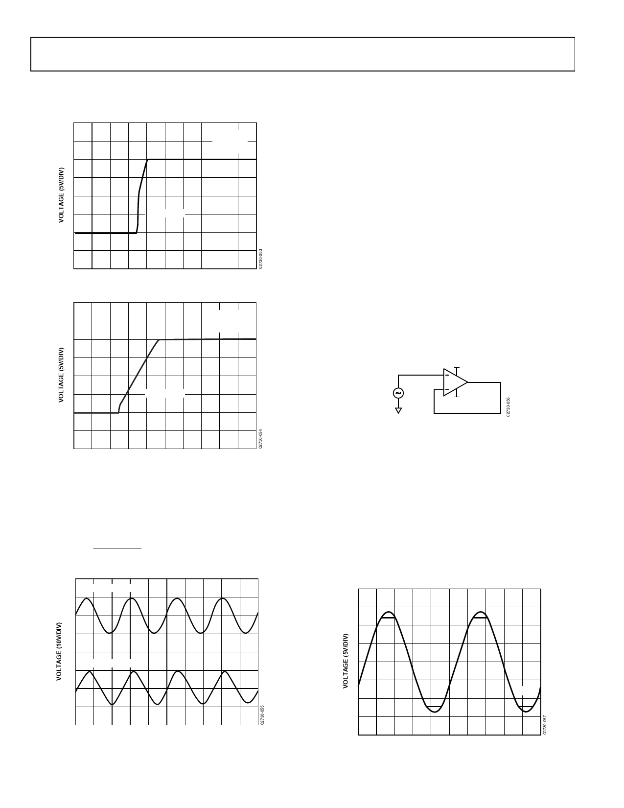
The slew rate of the AD8610/AD8620 is double that of the
OPA627 when configured in a unity gain of +1 (see Figure 53
and Figure 54).
VS = ±13V
RL = 2kΩ
G = +1
SR = 85V/µs
TIME (400ns/DIV)
Figure 53. +Slew Rate of AD8610/AD8620 in Unity Gain of +1
VS = ±13V
RL = 2kΩ
G = +1
SR = 23V/µs
TIME (400ns/DIV)
Figure 54. +Slew Rate of OPA627 in Unity Gain of +1
The slew rate of an amplifier determines the maximum frequency
at which it can respond to a large signal input. This frequency
(known as full-power bandwidth or FPBW) can be calculated
for a given distortion (for example, 1%) from the equation:
FPBW = SR
( ) 2π × VPEAK
CH1 = 20.8V p-p
0V
Input Overvoltage Protection
When the input of an amplifier is driven below VEE or above
VCC by more than one VBE, large currents flow from the sub
strate through the negative supply (V–) or the positive supply
(V+), respectively, to the input pins and can destroy the device.
If the input source can deliver larger currents than the maximum
forward current of the diode (>5 mA), a series resistor can be
added to protect the inputs. With its very low input bias and
offset current, a large series resistor can be placed in front of
the AD8610/AD8620 inputs to limit current to below damaging
levels. Series resistance of 10 kΩ generates less than 25 μV of offset.
This 10 kΩ allows input voltages more than 5 V beyond either
power supply. Thermal noise generated by the resistor adds
7.5 nV/√Hz to the noise of the AD8610/AD8620. For the AD8610/
AD8620, differential voltages equal to the supply voltage do not
cause any problem (see Figure 55). In this context, please note that
the high breakdown voltage of the input FETs eliminates the need
to include clamp diodes between the inputs of the amplifier, a prac-
tice that is mandatory on many precision op amps. Unfortunately,
clamp diodes greatly interfere with many application circuits
such as precision rectifiers and comparators. The AD8610/
AD8620 are free from these limitations.
V1
14V
0
+13V
3
7
6
2
4 AD8610
–13V
Figure 56. Unity Gain Follower
No Phase Reversal
Many amplifiers misbehave when one or both of the inputs are
forced beyond the input common-mode voltage range. Phase
reversal is typified by the transfer function of the amplifier, effect-
tively reversing its transfer polarity. In some cases, this can cause
lockup and even equipment damage in servo systems, and can
cause permanent damage or no recoverable parameter shifts to
the amplifier itself. Many amplifiers feature compensation cir-
cuitry to combat these effects, but some are only effective for
the inverting input. The AD8610/AD8620 are designed to prevent
phase reversal when one or both inputs are forced beyond their
input common-mode voltage range.
VIN
CH2 = 19.4V p-p
0V
TIME (400ns/DIV)
Figure 55. AD8610 FPBW
Rev. E | Page 16 of 24
VOUT
TIME (400µs/DIV)
Figure 57. No Phase Reversal
Share Link: 