X2N5432 Просмотр технического описания (PDF) - Calogic, LLC
Номер в каталоге
Компоненты Описание
производитель
X2N5432 Datasheet PDF : 2 Pages
| |||
N-Channel JFET Switch
2N5432 – 2N5434
FEATURES
Low rds(on)
• Excellent Switching
•• Low Cutoff Current
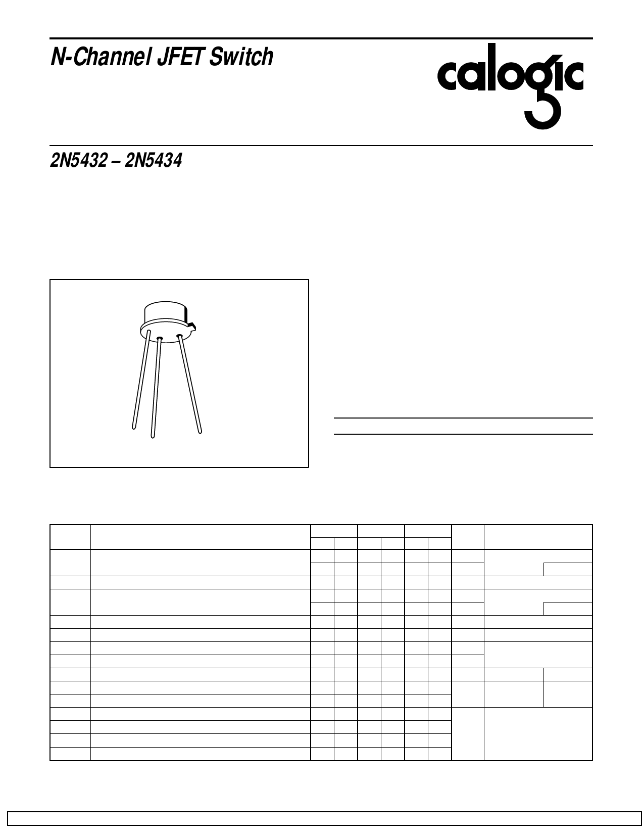
PIN CONFIGURATION
(TO-52)
5018
G, C
D
S
LLC
ABSOLUTE MAXIMUM RATINGS
(TA = 25oC unless otherwise noted)
Gate-Source Voltage . . . . . . . . . . . . . . . . . . . . . . . . . . . . -25V
Gate-Drain Voltage . . . . . . . . . . . . . . . . . . . . . . . . . . . . . -25V
Gate Current . . . . . . . . . . . . . . . . . . . . . . . . . . . . . . . . 100mA
Drain Current . . . . . . . . . . . . . . . . . . . . . . . . . . . . . . . . 400mA
Storage Temperature Range . . . . . . . . . . . . . -65oC to +200oC
Operating Temperature Range . . . . . . . . . . . -55oC to +150oC
Lead Temperature (Soldering, 10sec) . . . . . . . . . . . . . +300oC
Power Dissipation . . . . . . . . . . . . . . . . . . . . . . . . . . . . 300mW
Derate above 25oC . . . . . . . . . . . . . . . . . . . . . . . 2.3mW/oC
NOTE: Stresses above those listed under "Absolute Maximum
Ratings" may cause permanent damage to the device. These are
stress ratings only and functional operation of the device at these or
any other conditions above those indicated in the operational sections
of the specifications is not implied. Exposure to absolute maximum
rating conditions for extended periods may affect device reliability.
ORDERING INFORMATION
Part
Package
Temperature Range
2N5432-34 Hermetic TO-52
-55oC to +150oC
X2N5432-34 Sorted Chips in Carriers -55oC to +150oC
ELECTRICAL CHARACTERISTICS (TA = 25oC unless otherwise specified)
SYMBOL
PARAMETER
IGSS
BVGSS
ID(off)
VGS(off)
IDSS
rDS(on)
VDS(on)
rds(on)
Ciss
Crss
td
tr
toff
tf
Gate Reverse Current
Gate-Source Breakdown Voltage
Drain Cutoff Current
Gate-Source Cutoff Voltage
Saturation Drain Current (Note 1)
Static Drain-Source ON Resistance
Drain-Source ON Voltage
Drain-Source ON Resistance
Common-Source Input Capacitance (Note2)
Common-Source Reverse Transfer Capacitance (Note 2)
Turn-ON Delay Time (Note 2)
Rise Time (Note 2)
Turn-OFF Delay Time (Note 2)
Fall Time (Note 2)
2N5432 2N5433 2N5434
UNITS
MIN MAX MIN MAX MIN MAX
TEST CONDITIONS
-200
-200
-200
-200
-200 pA VGS = -15V, VDS = 0
-200 nA
TA = 150oC
-25
-25
-25
V IG = -1µA, VDS = 0
200
200
200 pA VDS = 5V, VGS = -10V
200
200
200 nA
TA = 150oC
-4 -10 -3 -9 -1 -4
V VDS = 5V, ID = 3nA
150
100
30
mA VDS = 15V, VGS = 0
25
50
7
10 ohm
VGS = 0, ID = 10mA
70
100 mV
5
7
10 ohm VGS = 0, ID = 0 f = 1kHz
30
15
30
15
30
15
pF
VDS = 0,
VGS = -10 V
f = 1MHz
4
4
4
1
1
1
VDD = 1.5V,
ns VGS(on) = 0,
6
6
6
VGS(off) = -12V,
30
30
30
ID(on) = 10mA
NOTES: 1. Pulse test required, pulsewidth 300µs, duty cycle ≤3%.
2. For design reference only, not 100% tested.
CALOGIC LLC, 237 WHITNEY PLACE, FREMONT, CA 94539, 510-656-2900 PHONE, 510-651-1076 FAX
DS009 REV A
Share Link: 