ADM1176(Rev0) –ü—Ä–æ—Å–º–æ—Ç—Ä —Ç–µ—Ö–Ω–∏—á–µ—Å–∫–æ–≥–æ –æ–ø–∏—Å–∞–Ω–∏—è (PDF) - Analog Devices
–ù–æ–º–µ—Ä –≤ –∫–∞—Ç–∞–ª–æ–≥–µ
–ö–æ–º–ø–æ–Ω–µ–Ω—Ç—ã –û–ø–∏—Å–∞–Ω–∏–µ
–ø—Ä–æ–∏–∑–≤–æ–¥–∏—Ç–µ–ª—å
ADM1176 Datasheet PDF : 24 Pages
| |||
ADM1176
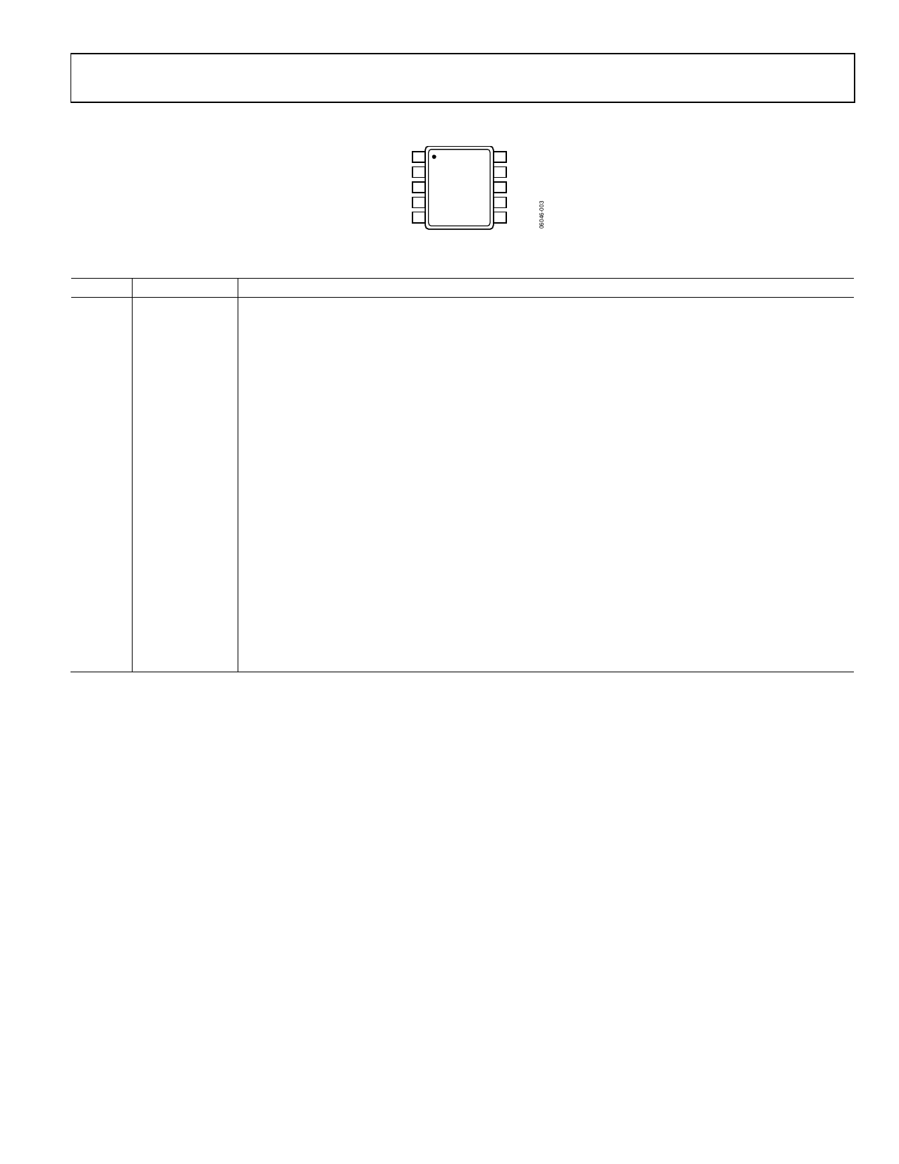
PIN CONFIGURATION AND FUNCTION DESCRIPTIONS
VCC 1
SENSE 2
ON 3
GND 4
TIMER 5
10 GATE
ADM1176
TOP VIEW
(Not to Scale)
9 A1
8 A0
7 SDA
6 SCL
Figure 3. Pin Configuration
Table 4. Pin Function Descriptions
Pin No. Mnemonic
Description
1
VCC
Positive Supply Input Pin. The operating supply voltage range is from 3.15 V to 16.5 V. An undervoltage
lockout (UVLO) circuit resets the ADM1176 when a low supply voltage is detected.
2
SENSE
Current Sense Input Pin. A sense resistor between the VCC pin and the SENSE pin sets the analog current
limit. The hot swap operation of the ADM1176 controls the external FET gate to maintain the (VVCC ‚àí VSENSE)
voltage at 100 mV or below.
3
ON
Undervoltage Input Pin. Active-high pin. An internal ON comparator has a trip threshold of 1.3 V, and the
output of this comparator is used as an enable for the hot swap operation. With an external resistor divider
from VCC to GND, this pin can be used to enable the hot swap operation on a specific voltage on VCC, giving
an undervoltage function.
4
GND
Chip Ground Pin.
5
TIMER
Timer Pin. An external capacitor, CTIMER, sets a 270 ms/μF initial timing cycle delay and a 21.7 ms/μF fault delay.
The GATE pin turns off when the TIMER pin is pulled beyond the upper threshold. An overvoltage detection
with an external Zener can be used to force this pin high.
6
SCL
I2C Clock Pin. Open-drain input requires an external resistive pull-up.
7
SDA
I2C Data I/O Pin. Open-drain input/output. Requires an external resistive pull-up.
8
A0
I2C Address Pin. This pin can be tied low, tied high, left floating, or tied low through a resistor. Sixteen different
I2C address options are available, depending on the external configuration of the A0 pin and A1 pin.
9
A1
I2C Address Pin. This pin can be tied low, tied high, left floating or tied low through a resistor. Sixteen different
I2C address options are available, depending on the external configuration of the A0 pin and the A1 pin.
10
GATE
GATE Output Pin. This pin is the high-side gate drive of an external N-channel FET. This pin is driven by the
FET drive controller, which utilizes a charge pump to provide a 12.5 μA pull-up current to charge the FET
GATE pin. The FET drive controller regulates to a maximum load current (100 mV through the sense resistor)
by modulating the GATE pin.
Rev. 0 | Page 7 of 24
Share Link: 