APL3205AQBI-TRG Просмотр технического описания (PDF) - Anpec Electronics
Номер в каталоге
Компоненты Описание
производитель
APL3205AQBI-TRG Datasheet PDF : 20 Pages
| |||
APL3205A/B
Application Information
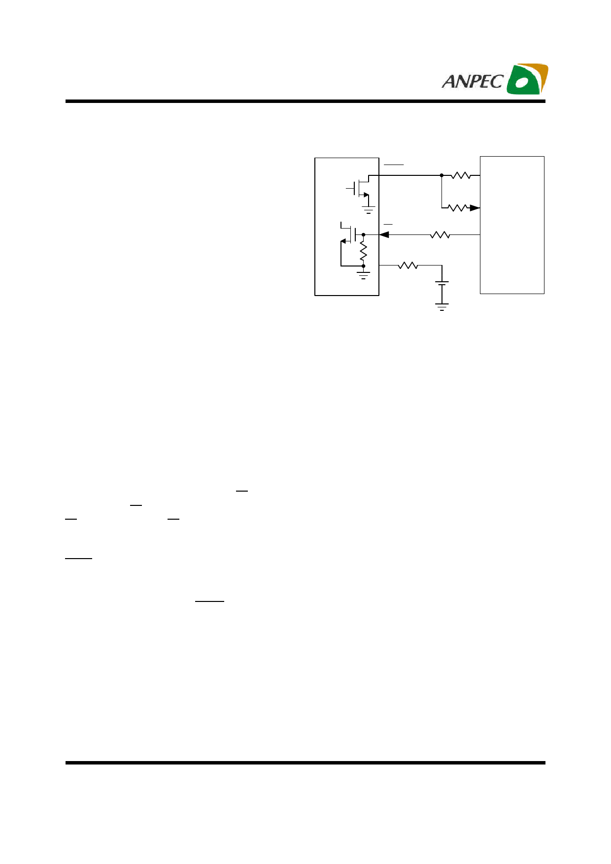
RBAT Selection
Connect the BAT pin to the positive terminal of battery
through a resistor RBAT for battery OVP function. The RBAT
limits the current flowing from BAT to battery in case of
BAT pin is shortened to VIN pin under a failure mode. The
recommended
value
of
R
BAT
is
100kΩ.
In
the
worse
case
of an IC failure, the current flowing from the BAT pin to the
battery is:
(30V-3V)/ 100kΩ =270µA
where the 30V is the maximum IN voltage and the 3V is
the minimum battery voltage. The current is so small that
can be absorbed by the charger system.
The disadvantage with the large R is that the error of
BAT
the battery OVP threshold will be increased. The addi-
tional error is the voltage drop across the RBAT because
of
the
BAT
bias
current.
When
R
BAT
is
100kΩ,
the
worse-
case additional error is 100kΩx20nA=2mV, which is ac-
ceptable in most applications.
REN Selection
For the same reason as the BAT pin case, the EN pin
should be connected to the MCU GPIO pin through a
resistor. The value of the REN is dependent on the IO
voltage of the MCU.
Since the IO voltage is divided by R and EN internal pull
EN
low resistor for EN voltage. It has to be ensured that the
EN voltage is above the EN logic high voltage when the
GPIO output of the MCU is high.
FAULT Output
Since the FAULT pin is an open-drain output, connecting
a resistor RUP to a pull high voltage is necessary. It is also
recommended that connect the FAULT to the MCU GPIO
through a resistor R . The R prevents damage to
FAULT
FAULT
the MCU under a failure mode. The recommended value
of the resistors should be between 10kΩ and 100kΩ.
FAULT
EN
BAT RBAT
RUP
RFAULT
REN
VIO
GPIO
MCU
GPIO
Li+ Battery
Figure 6. RUP, RFAULT, REN and RBAT
Capacitor Selection
The input capacitor is for decoupling and prevents the
input voltage from overshooting to dangerous levels. In
the AC adapter hot plug-in applications or load current
step-down transient, the input voltage has a transient
spike due to the parasitic inductance of the input cable. A
25V, X5R, dielectric ceramic capacitor with a value be-
tween 1µF and 4.7µF placed close to the IN pin is
recommended.
The output capacitor is for output voltage decoupling, and
also can be as the input capacitor of the charging circuit.
At least, a 1µF, 10V, X5R capacitor is recommended.
Layout Consideration
In some failure modes, a high voltage may be applied to
the device. Make sure that the clearance constraint of the
PCB layout must satisfy the design rule for high voltage.
The exposed pad of the TDFN2x2-8 performs the func-
tion of channeling heat away. It is recommended that
connect the exposed pad to a large copper ground plane
on the backside of the circuit board through several ther-
mal vias to improve heat dissipation.
The input and output capacitors should be placed close
to the IC. R also should be placed close to the IC.
ILIM
The high current traces like input trace and output trace
must be wide and short.
Copyright © ANPEC Electronics Corp.
15
Rev. A.2 - May., 2009
www.anpec.com.tw
Share Link: 