AS7C256A-15JI Просмотр технического описания (PDF) - Alliance Semiconductor
Номер в каталоге
Компоненты Описание
производитель
AS7C256A-15JI Datasheet PDF : 9 Pages
| |||
AS7C256A
®
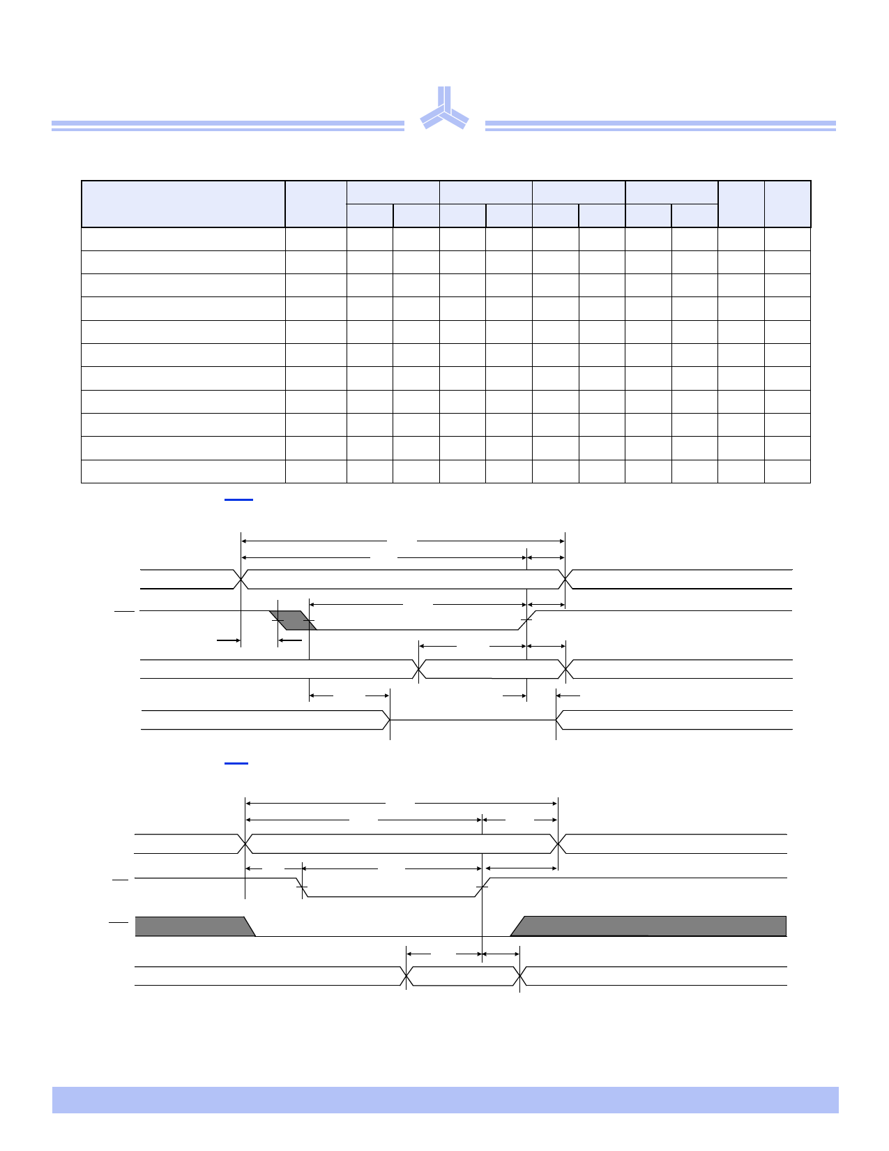
Write cycle (over the operating range)9
-10
Parameter
Symbol Min Max
Write cycle time
tWC
10
–
Chip enable to write end
tCW
8
–
Address setup to write end
tAW
8
–
Address setup time
tAS
0
–
Write pulse width
tWP
7
–
Write recovery time
tWR
0
–
Address hold from end of write
tAH
0
–
Data valid to write end
tDW
5
–
Data hold time
tDH
0
–
Write enable to output in high Z tWZ
–
5
Output active from write end
tOW
3
–
-12
Min Max
12 –
8
–
8
–
0
–
8
–
0
–
0
–
6
–
0
–
–
6
3
–
-15
Min Max
15 –
10 –
10 –
0
–
9
–
0
–
0
–
8
–
0
–
–
7
3
–
-20
Min Max
20 –
12 –
12 –
0
–
12 –
0
–
0
–
10 –
0
–
–
8
3
–
Unit Notes
ns
ns
ns
ns
ns
ns
ns
ns
ns 3,4
ns 3,4
ns 3,4
Write waveform 1 (WE controlled)9
Address
tWC
tAW
tWP
WE
tAS
Din
tWZ
Dout
tAH
tWR
tDW
tDH
Data valid
tOW
Write waveform 2 (CE controlled)9
tWC
tAW
Address
CE
tAS
tCW
tAH
tWR
WE
tDW
tDH
Din
Data valid
9/24/04; v.1.2
Alliance Semiconductor
P. 5 of 9
Share Link: 