CA3290 Просмотр технического описания (PDF) - Intersil
Номер в каталоге
Компоненты Описание
производитель
CA3290 Datasheet PDF : 10 Pages
| |||
CA3290, CA3290A
Absolute Maximum Ratings
Supply Voltage
Single Supply . . . . . . . . . . . . . . . . . . . . . . . . . . . . . . . . . . . . .+36V
Dual Supply . . . . . . . . . . . . . . . . . . . . . . . . . . . . . . . . . . . . . . . . . . ±18V
Differential Input Voltage . . . . . . . . . . . . . . . . 36V or [(V+ - V-) +5V]
(whichever is less)
DC Input Voltage . . . . . . . . . . . . . . . . . . . . . . . . . . V+ +5V to V- -5V
Output to V- Short Circuit Duration (Note 1) . . . . . . . . . . Continuous
Input Current . . . . . . . . . . . . . . . . . . . . . . . . . . . . . . . . . . . . . . . 1mA
Thermal Information
Thermal Resistance (Typical, Note 2)
θJA (oC/W) θJC (oC/W)
PDIP Package . . . . . . . . . . . . . . . . . . . 110
N/A
Maximum Junction Temperature (Plastic Package) . . . . . . . .150oC
Maximum Storage Temperature Range . . . . . . . . . -65oC to 150oC
Maximum Lead Temperature (Soldering 10s) . . . . . . . . . . . . 300oC
Operating Conditions
Temperature Range. . . . . . . . . . . . . . . . . . . . . . . . . . . -55 to 125oC
CAUTION: Stresses above those listed in “Absolute Maximum Ratings” may cause permanent damage to the device. This is a stress only rating and operation of the
device at these or any other conditions above those indicated in the operational sections of this specification is not implied.
NOTES:
1. Short circuits from the output to V+ can cause excessive heating and eventual destruction of the device.
2. θJA is measured with the component mounted on an evaluation PC board in free air.
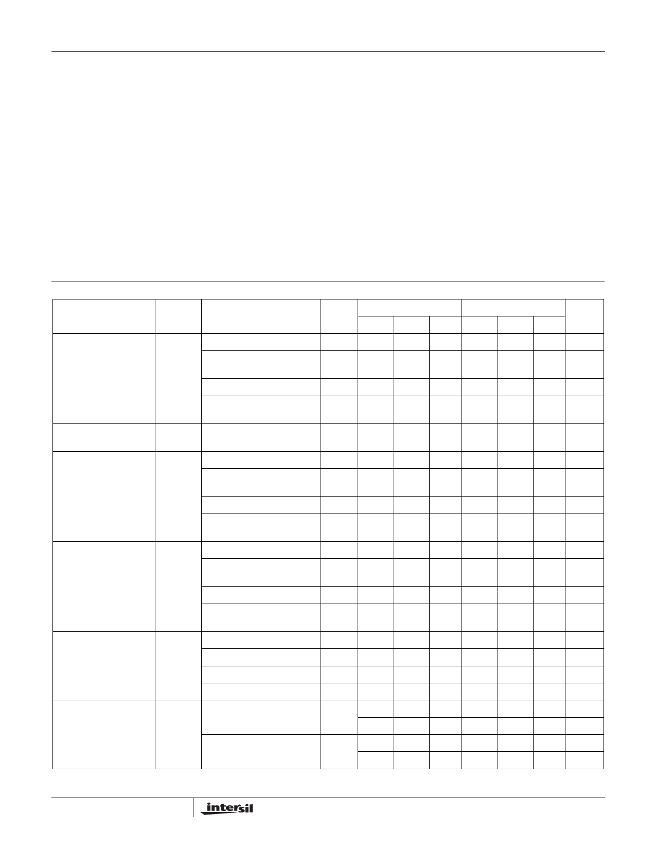
Electrical Specifications V- = 0V, Unless Otherwise Specified
PARAMETER
SYMBOL
TEST CONDITIONS
TEMP
(oC)
CA3290A
MIN TYP MAX
CA3290
MIN TYP MAX UNITS
Input Offset Voltage
VIO VCM = VO = 1.4V, V+ = 5V
Full
-
4.5
-
VCM = VO = 0V, V+ = +15V,
Full
-
8.5
-
V- = -15V
-
8.5
-
mV
-
8.5
-
mV
VCM = VO = 1.4V, V+ = 5V
25
VCM = VO = 0V, V+ = +15V,
25
V- = -15V
Temperature Coefficient ∆VIO/∆T
of Input Offset Voltage
-
4.0
10
-
-
4.0
10
-
-
8
-
-
7.5
20
mV
7.5
20
mV
8
-
µV/oC
Input Offset Current
IIO
VCM = 1.4V, V+ = 5V
Full
-
VCM = 0V, V+ = +15V, V- = -
Full
-
15V
2
28
-
7
28
-
2
32
nA
7
32
nA
VCM = 1.4V, V+ = 5V
VCM = 0V,
V+ = +15V, V- = -15V
25
-
25
-
2
25
-
7
25
-
2
30
pA
7
30
pA
Input Current
II
VCM = 1.4V, V+ = 5V
125
-
2.8
45
-
2.8
55
nA
VCM = 0V, V+ = +15V, V- = -
125
-
13
45
-
13
55
nA
15V
VCM = 1.4V, V+ = 5V
25
VCM = 0V, V+ = +15V, V- = -
25
15V
-
3.5
40
-
-
12
40
-
3.5
50
pA
12
50
pA
Supply Current
Voltage Gain
I+
RL = ∞, V+ = 5V
RL = ∞, V+ = 30V
RL = ∞, V+ = 5V
RL = ∞, V+ = 30V
AOL RL = 15kΩ, V+ = +15V,
V- = -15V
-55
-
0.85 1.0
-
0.85 1.6
mA
-55
-
1.62 3.0
-
1.62 3.5
mA
25
-
0.8
1.4
-
0.8
1.4
mA
25
-
1.35 3.0
-
1.35 3.0
mA
Full
-
150
-
-
150
-
V/mV
-
103
-
-
103
-
dB
RL = 15kΩ, V+ = +15V,
V- = -15V
25
25
800
-
25
800
-
V/mV
88
118
-
88
118
-
dB
2
Share Link: 