UPD78083 Просмотр технического описания (PDF) - NEC => Renesas Technology
Номер в каталоге
Компоненты Описание
производитель
UPD78083 Datasheet PDF : 62 Pages
| |||
µPD78001B(A), 78002B(A)
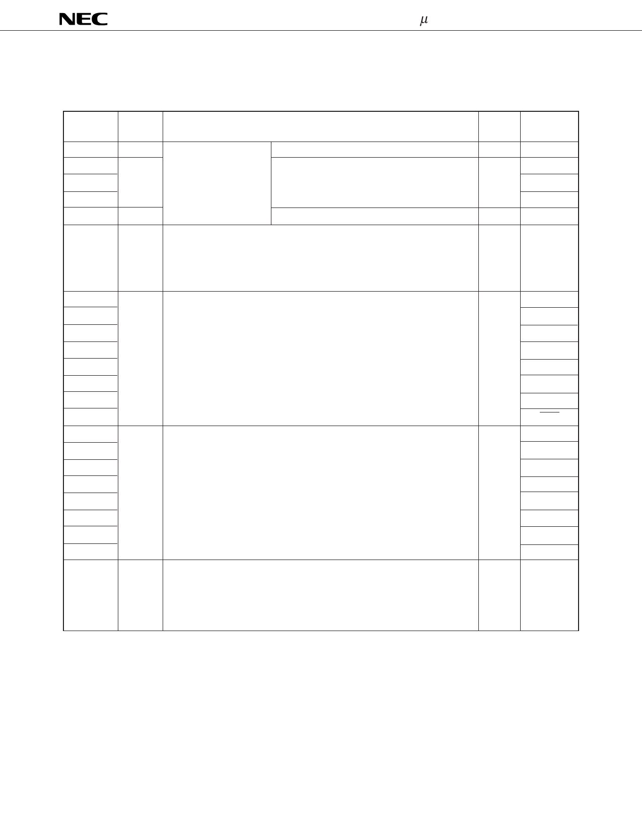
3. PIN FUNCTIONS
3.1 PORT PINS (1/2)
Pin Name
I/O
P00
P01
P02
P03
P04*
P10 to P17
Input
Input/
output
Input
Input/
output
Port 0
5-bit I/O port
Function
Input only
Input/output can be specified bit-wise.
When used as an input port, pull-up resistor can
be used by software.
Input only
Port 1
8-bit input/output port.
Input/output can be specified bit-wise.
When used as an input port, pull-up resistor can be used by software.
After
Reset
Input
Input
Input
Dual-
Function Pin
INTP0
INTP1
INTP2
INTP3
XT1
–
P20
P21
P22
P23
P24
P25
P26
P27
P30
P31
P32
P33
P34
P35
P36
P37
P40 to P47
Input/
output
Input/
output
Input/
output
Port 2
8-bit input/output port.
Input/output can be specified bit-wise.
When used as an input port, pull-up resistor can be used by software.
Port 3
8-bit input/output port.
Input/output can be specified in bit-wise.
When used as an input port, pull-up resistor can be used by software.
Port 4
8-bit input/output port.
Input/output can be specified in 8-bit unit.
When used as an input port, pull-up resistor can be used by software.
Test input flag (KRIF) is set to 1 by falling edge detection.
Input
Input
Input
–
–
–
–
–
SI0/SB0
SO0/SB1
SCK0
–
TO1
TO2
TI1
TI2
PCL
BUZ
–
AD0 to AD7
* When using the P04/XT1 pins as an input port, set 1 to bit 6 (FRC) of the processor control register. (Do not use
the on-chip feedback register of the subsystem clock oscillator.)
10
Share Link: 