HA17901AT Просмотр технического описания (PDF) - Renesas Electronics
Номер в каталоге
Компоненты Описание
производитель
HA17901AT Datasheet PDF : 16 Pages
| |||
HA17901A Series
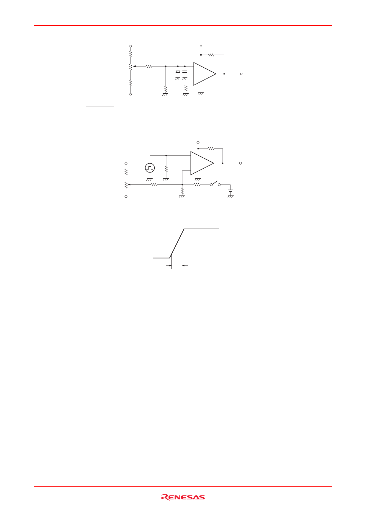
4. Voltage gain (AV) test circuit (RL = 15 kΩ)
+V
VCC
20k
Vin
RL 15k
10k
30k
+
10µ −
+
20k
−
VO
50 50
−V
AV
=
20
log
VO1
VIN1
−
−
VO2
VIN2
(dB)
5. Response time (tR) test circuit
VCC
+V Vin
24k
50
P.G
VR
5k
30k
50
−V
− RL 5.1k
+
120k SW
VO
12V
tR: RL = 5.1 kΩ, a 100 mV input step voltage that has a 5 mV overdrive
With VIN not applied, set the switch SW to the off position and adjust VR so that VO is in the vicinity of 1.4 V.
Apply VIN and turn the switch SW on.
90%
10%
tR
Rev.1.00 Mar 10, 2006 page 6 of 15
Share Link: 