AD8306ARZ Просмотр технического описания (PDF) - Analog Devices
Номер в каталоге
Компоненты Описание
производитель
AD8306ARZ Datasheet PDF : 16 Pages
| |||
ABSOLUTE MAXIMUM RATINGS*
Supply Voltage VS . . . . . . . . . . . . . . . . . . . . . . . . . . . . . . 7.5 V
Input Level, Differential (re 50 Ω) . . . . . . . . . . . . . . . +26 dBm
Input Level, Single-Ended (re 50 Ω) . . . . . . . . . . . . . +20 dBm
Internal Power Dissipation . . . . . . . . . . . . . . . . . . . . . 800 mW
θJA . . . . . . . . . . . . . . . . . . . . . . . . . . . . . . . . . . . . . . . 125°C/W
θJC . . . . . . . . . . . . . . . . . . . . . . . . . . . . . . . . . . . . . . . . 25°C/W
Maximum Junction Temperature . . . . . . . . . . . . . . . . +125°C
Operating Temperature Range . . . . . . . . . . . . –40°C to +85°C
AD8306
Storage Temperature Range
–65°C to +150°C
Lead Temperature Range (Soldering 60 sec)
+300°C
*Stresses above those listed under Absolute Maximum Ratings may cause perma-
nent damage to the device. This is a stress rating only; functional operation of the
device at these or any other conditions above those indicated in the operational
section of this specification is not implied. Exposure to absolute maximum rating
conditions for extended periods may effect device reliability.
Model
AD8306AR
AD8306AR-REEL
AD8306AR-REEL7
AD8306ACHIPS
5962-9864601QEA
AD8306-EVAL
Temperature
Range
–40°C to +85°C
–40°C to +85°C
–40°C to +85°C
–40°C to +85°C
–55°C to +125°C
ORDERING GUIDE
Package
Description
16-Lead Narrow Body SO
13" Tape and Reel
7" Tape and Reel
Die
16-Lead Side-Brazed Ceramic DIP
Evaluation Board
Package
Options
SO-16
SO-16
SO-16
D-16
CAUTION
ESD (electrostatic discharge) sensitive device. Electrostatic charges as high as 4000 V readily
accumulate on the human body and test equipment and can discharge without detection.
Although the AD8306 features proprietary ESD protection circuitry, permanent damage may
occur on devices subjected to high energy electrostatic discharges. Therefore, proper ESD
precautions are recommended to avoid performance degradation or loss of functionality.
WARNING!
ESD SENSITIVE DEVICE
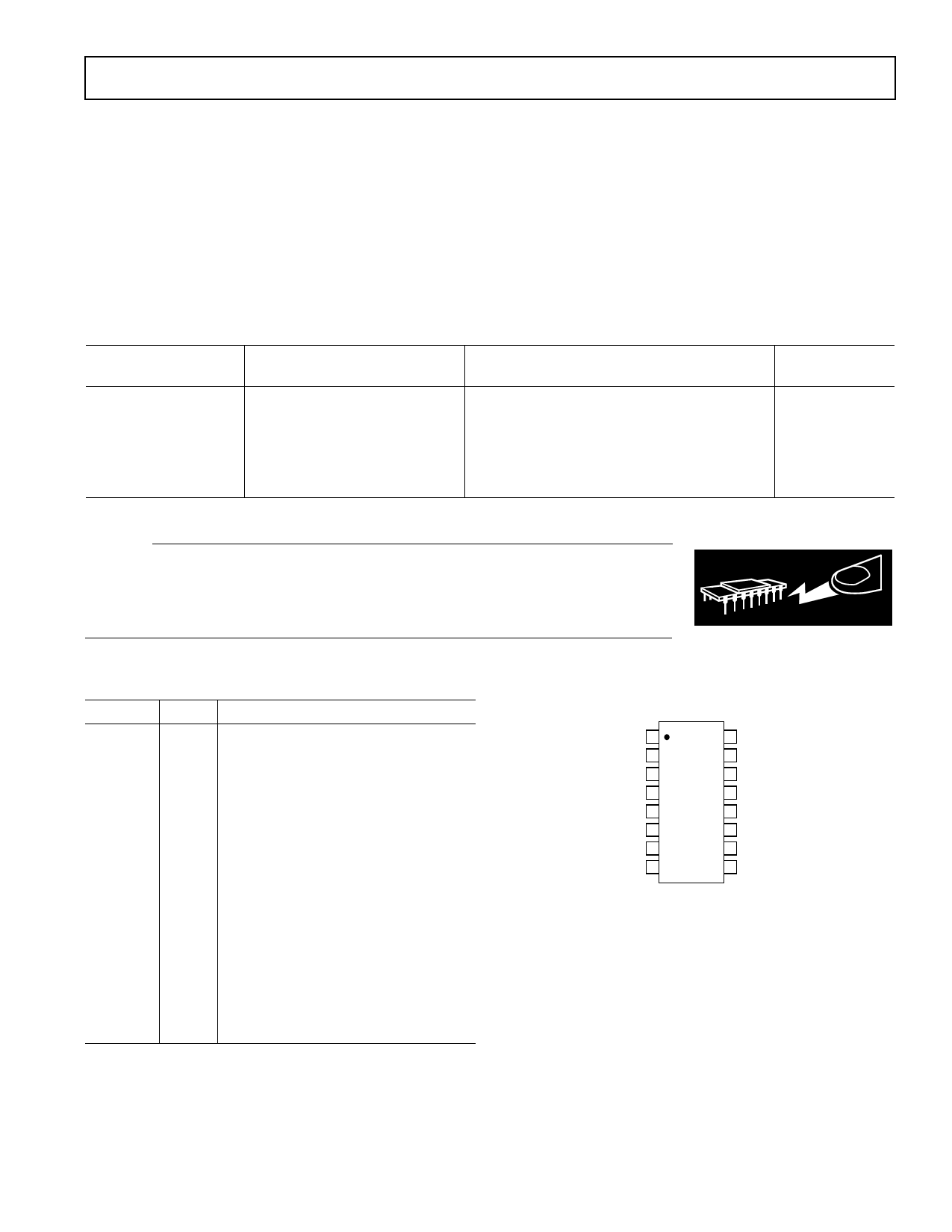
PIN FUNCTION DESCRIPTIONS
Pin
Name Function
1
COM2 Special Common Pin for RSSI Output.
2
VPS1 Supply Pin for First Five Amplifier Stages
and the Main Biasing System.
3, 6, 11, 14 PADL Four Tie-Downs to the Paddle on
which the IC Is Mounted; Grounded.
4
INHI Signal Input, HI or Plus Polarity.
5
INLO Signal Input, LO or Minus Polarity.
7
COM1 Main Common Connection.
8
ENBL Chip Enable; Active When HI.
9
LMDR Limiter Drive Programming Pin.
10
FLTR RSSI Bandwidth-Reduction Pin.
12
LMLO Limiter Output, LO or Minus Polarity.
13
LMHI Limiter Output, HI or Plus Polarity.
15
VPS2 Supply Pin for Sixth Gain Stage, Limiter
and RSSI Output Stage Load Current.
16
VLOG Logarithmic (RSSI) Output.
PIN CONFIGURATION
COM2 1
16 VLOG
VPS1 2
15 VPS2
PADL 3
14 PADL
INHI 4 AD8306 13 LMHI
INLO
5
TOP VIEW
(Not to Scale) 12
LMLO
PADL 6
11 PADL
COM1 7
10 FLTR
ENBL 8
9 LMDR
REV. A
–3–
Share Link: 