LTC3405 Просмотр технического описания (PDF) - Linear Technology
Номер в каталоге
Компоненты Описание
производитель
LTC3405 Datasheet PDF : 20 Pages
| |||
LT3420/LT3420-1
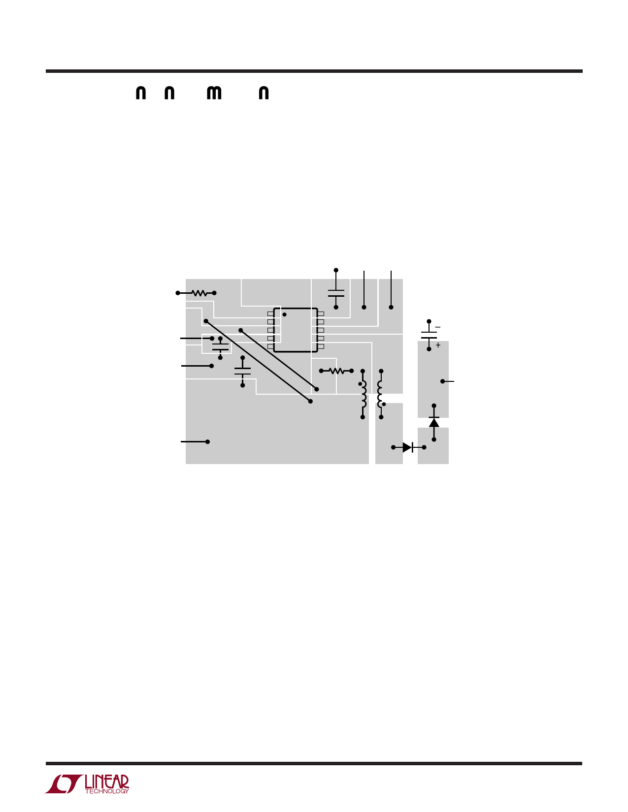
APPLICATIO S I FOR ATIO
BOARD LAYOUT
The high voltage operation of the LT3420/LT3420-1
demands careful attention to board layout. You will not
get advertised performance with careless layout. Fig-
ure␣ 11 shows the recommended component placement.
Keep the area for the high voltage end of the secondary
as small as possible. Note the larger than minimum
spacing for all high voltage nodes. This is necessary to
meet the breakdown specifications for the circuit board.
If the Photoflash capacitor is placed far from the LT3420/
LT3420-1 circuit, place a small (20nF-50nF) ceramic
capacitor with sufficient voltage rating close to the part.
This insures adequate bypassing. Remember that
LETHAL VOLTAGES ARE PRESENT in this circuit. Use
caution when working with the circuit.
R2
VCC
C2
GND
C1
CHARGE DONE
C3
PHOTOFLASH
CAPACITOR
R1
T1
VOUT
VBAT
D1B
D1A
3420 F11
Figure 11. Suggested Layout
3420fa
15
Share Link: 