MAX15029 Просмотр технического описания (PDF) - Maxim Integrated
Номер в каталоге
Компоненты Описание
производитель
MAX15029 Datasheet PDF : 12 Pages
| |||
MAX15029/MAX15030
1.425V to 3.6V Input, 500mA Low-Dropout
Regulators with BIAS Input
Absolute Maximum Ratings
IN, FB, SS, I.C. to GND........................................-0.3V to +4.0V
BIAS to GND............................................................-0.3V to +6V
EN to GND..............-0.3V to the lower of (VBIAS + 0.3V) or +6V
OUT to GND................................................-0.3V to (VIN + 0.3V)
Output Short-Circuit Duration.....................................Continuous
Continuous Power Dissipation (TA = +70°C)
TDFN (derate 24.4mW/°C above +70°C)...................1951mW
Operating Junction Temperature Range........... -40°C to +125°C
Maximum Junction Temperature......................................+150°C
Storage Temperature Range............................. -65°C to +150°C
Lead Temperature (soldering, 10s).................................. +300°C
Soldering Temperature (reflow)........................................+260°C
Stresses beyond those listed under “Absolute Maximum Ratings” may cause permanent damage to the device. These are stress ratings only, and functional operation of the device at these
or any other conditions beyond those indicated in the operational sections of the specifications is not implied. Exposure to absolute maximum rating conditions for extended periods may affect
device reliability.
Package Thermal Characteristics (Note 1)
TDFN
Junction-to-Ambient Thermal Resistance (θJA)...........41°C/W
Junction-to-Case Thermal Resistance (θJC)..................9°C/W
Side-Wettable TDFN
Junction-to-Ambient Thermal Resistance (θJA)...........41°C/W
Junction-to-Case Thermal Resistance (θJC)..................8°C/W
Note 1: Package thermal resistances were obtained using the method described in JEDEC specification JESD51-7, using a four-layer
board. For detailed information on package thermal considerations, refer to www.maximintegrated.com/thermal-tutorial.
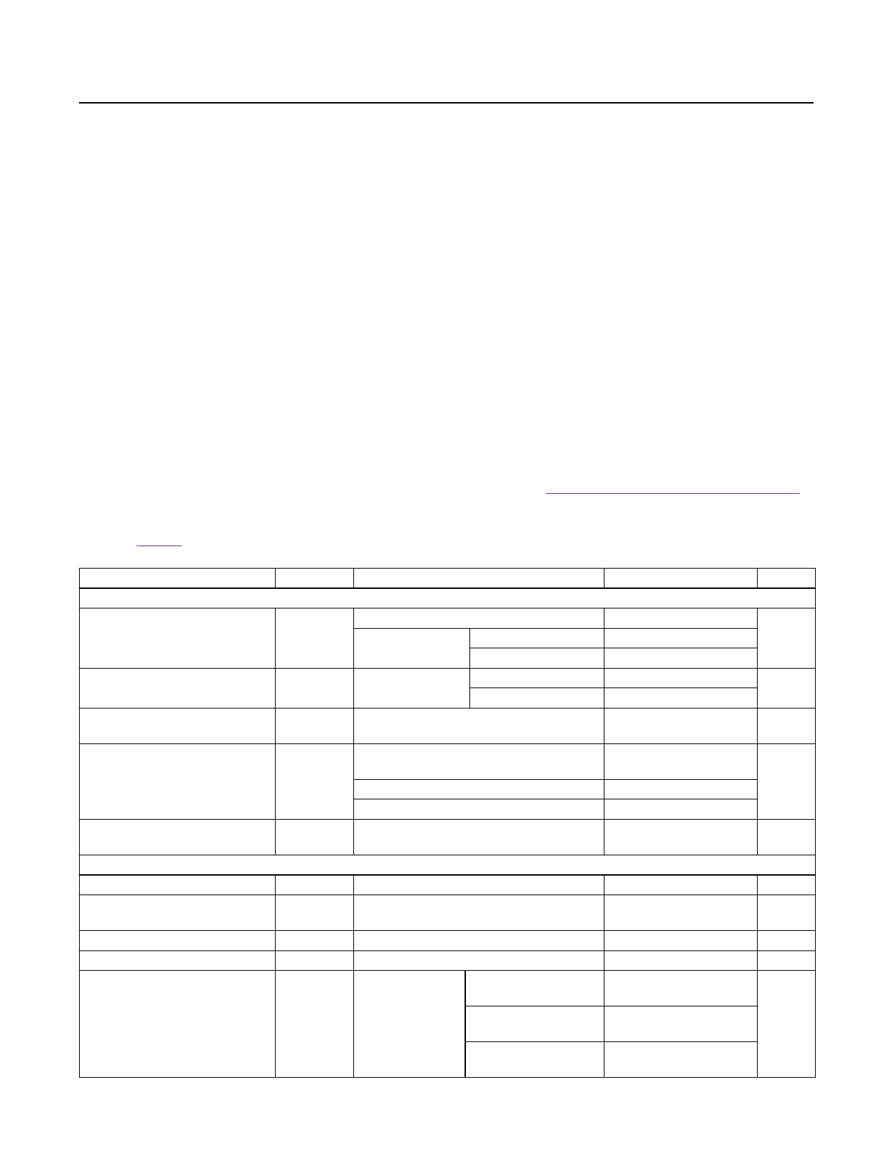
Electrical Characteristics
(Circuit of Figure 1; VIN = 1.8V, VOUT = 1.2V, EN = IN for MAX15029, EN = BIAS for MAX15030, IOUT = 100mA, TA = TJ = -40°C to
+125°C. Typical values are at TA = +25°C, unless otherwise noted.) (Note 2)
PARAMETER
SYMBOL
CONDITIONS
MIN TYP MAX UNITS
IN
MAX15029
1.425
3.600
Input Voltage Range
VIN
MAX15030
VBIAS = 3V to 5.5V
BIAS = IN
1.425
3.000
3.600
V
3.600
Undervoltage Lockout
VUVLO VIN rising
MAX15029
MAX15030
1.275 1.325 1.375
V
1.04 1.09 1.14
Undervoltage Lockout
Hysteresis
Quiescent GND Current
Input Supply Current in
Shutdown
VUVLO_
HYST
IGND
IIN_SD
IOUT = 2mA
VIN = 1.425V to 3.6V, VOUT = 1.2V,
IOUT = 1mA, VBIAS = 3.3V
VIN = 3.6V, VOUT = 3.3V, IOUT = 100mA
VIN = 3.3V, VOUT = 3.3V, IOUT = 500mA
VEN = 0V (TA = -40°C to +85°C)
50
mV
160 275 410
180 325 560
µA
170 315 470
0.1
5.5
µA
BIAS (MAX15030)
Input Voltage Range
Undervoltage Lockout
Undervoltage Lockout Hysteresis
Quiescent Input Supply Current
VBIAS
VBIAS_
UVLO
IBIAS
VBIAS rising
IOUT = 2mA
VEN = VBIAS
Input Supply Current in
Shutdown
IBIAS_SD EN = GND
3
5.5
V
2.3
2.5
2.7
V
110
mV
20
60
120
µA
VIN = 0V, VOUT = 0V,
VBIAS = 3.3V
VIN = 3.3V, VOUT = 0V,
VBIAS = 3.3V
VIN = 3.3V, VOUT = 0V,
VBIAS = 5V
1.2
2
1.2
2
µA
1.5
3
www.maximintegrated.com
Maxim Integrated │ 2
Share Link: 