MC100E157 Просмотр технического описания (PDF) - ON Semiconductor
Номер в каталоге
Компоненты Описание
производитель
MC100E157 Datasheet PDF : 8 Pages
| |||
MC10E157, MC100E157
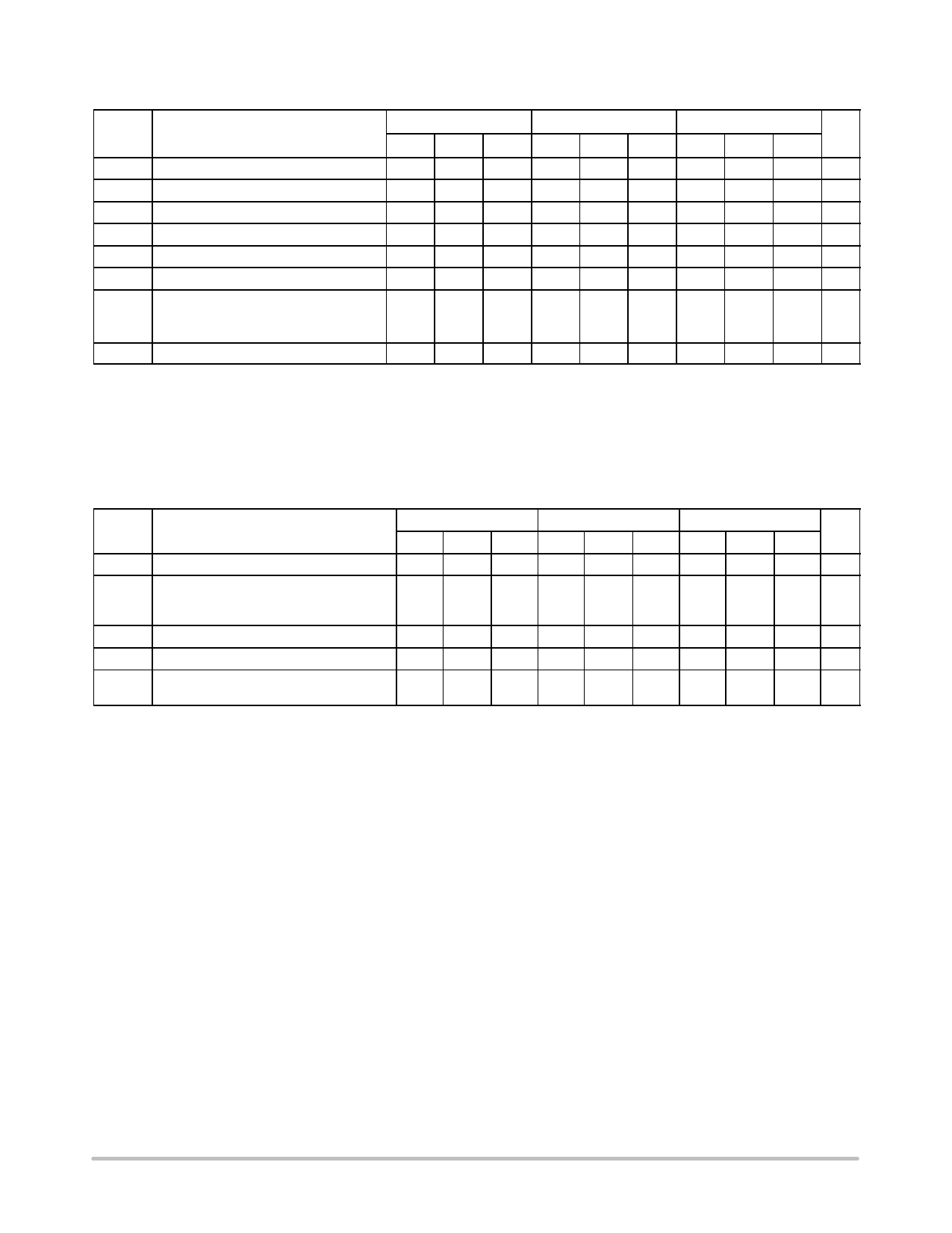
Table 7. 100E SERIES NECL DC CHARACTERISTICS VCCx = 0 V; VEE = −5.0 V (Note 7)
0°C
25°C
85°C
Symbol
Characteristic
Min Typ Max Min Typ Max Min Typ Max Unit
IEE
Power Supply Current
32
38
32
38
37
44 mA
VOH
Output HIGH Voltage (Note 8)
−1025 −950 −880 −1025 −950 −880 −1025 −950 −880 mV
VOL
Output LOW Voltage (Note 8)
−1810 −1705 −1620 −1810 −1745 −1620 −1810 −1740 −1620 mV
VIH
Input HIGH Voltage
−1165 −1025 −880 −1165 −1025 −880 −1165 −1025 −880 mV
VIL
Input LOW Voltage
−1810 −1645 −1475 −1810 −1645 −1475 −1810 −1645 −1475 mV
VBB
Output Voltage Reference
−1.38
−1.26 −1.38
−1.26 −1.38
−1.26 V
IIH
Input HIGH Current
D
200
200
200 mA
SEL
150
150
150 mA
IIL
Input LOW Current
0.5 0.3
0.5 0.25
0.5 0.2
mA
NOTE: Device will meet the specifications after thermal equilibrium has been established when mounted in a test socket or printed circuit
board with maintained transverse airflow greater than 500 lfpm. Electrical parameters are guaranteed only over the declared
operating temperature range. Functional operation of the device exceeding these conditions is not implied. Device specification limit
values are applied individually under normal operating conditions and not valid simultaneously.
7. Input and output parameters vary 1:1 with VCC. VEE can vary −0.46 V / +0.8 V.
8. Outputs are terminated through a 50 W resistor to VCC − 2.0 V.
Table 8. AC CHARACTERISTICS VCCx= 5.0 V; VEE = 0.0 V or VCCx = 0.0 V; VEE = −5.0 V (Note 9)
0°C
25°C
85°C
Symbol
fMAX
tPLH
tPHL
Characteristic
Maximum Toggle Frequency
Propagation Delay to Output
Min Typ Max Min Typ Max Min Typ Max Unit
700 1100
700 1100
700 1100
MHz
ps
D 220 380 550 220 380 550 220 380 550
SEL 425 600 800 425 600 800 425 600 800
tSKEW
tJITTER
tr
tf
Within-Device Skew (Note 10)
Random Clock Jitter (RMS)
Rise/Fall Time
(20 - 80%)
70
70
70
ps
<1
<1
<1
ps
ps
275 400 650 275 400 650 275 400 650
NOTE: Device will meet the specifications after thermal equilibrium has been established when mounted in a test socket or printed circuit
board with maintained transverse airflow greater than 500 lfpm. Electrical parameters are guaranteed only over the declared
operating temperature range. Functional operation of the device exceeding these conditions is not implied. Device specification limit
values are applied individually under normal operating conditions and not valid simultaneously.
9. 10 Series: VEE can vary −0.46 V / +0.06 V.
100 Series: VEE can vary −0.46 V / +0.8 V.
10. Within-device skew is defined as identical transitions on similar paths through a device.
http://onsemi.com
5
Share Link: 