MC10H350FNG(2016) Просмотр технического описания (PDF) - ON Semiconductor
Номер в каталоге
Компоненты Описание
производитель
MC10H350FNG Datasheet PDF : 6 Pages
| |||
9
3
4
2
5
6
7
11
12
10
13
14
15
VCC (+5.0 VDC) = PINS 1 AND 16
GND = PIN 8 (DIP)
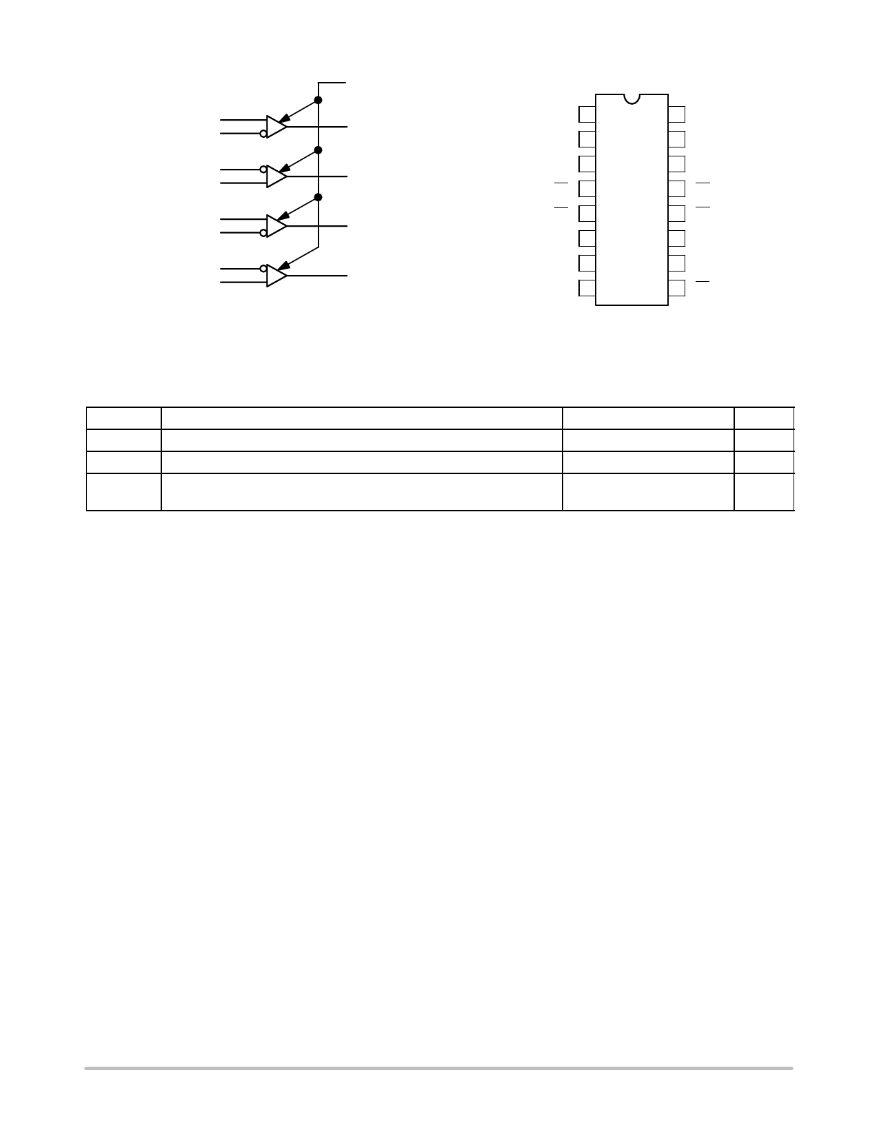
Figure 1. Logic Diagram
MC10H350
ECL VCC
1
AOUT
2
AIN
3
AIN
4
BIN
5
BIN
6
BOUT
7
GND
8
16
TTL VCC
15
COUT
14
CIN
13
CIN
12
DIN
11
DIN
10
DOUT
9
OE
3 2 1 20 19
AIN 4
AIN 5
NC 6
MC10H350
18 CIN
17 CIN
16 NC
BIN 7
BIN 8
15 DIN
14 DIN
9 10 11 12 13
Pin assignment is for Dual-in-Line Package.
Figure 2. Dip Pin Assignment
Figure 3. PLCC−20 Pin Assignment
Table 1. MAXIMUM RATINGS
Symbol
Characteristic
Rating
Unit
VCC
Power Supply (VEE = GND)
TA
Operating Temperature Range
Tstg
Storage Temperature Range
− Plastic
7.0
Vdc
0 to +75
°C
°C
−55 to +150
Stresses exceeding those listed in the Maximum Ratings table may damage the device. If any of these limits are exceeded, device functionality
should not be assumed, damage may occur and reliability may be affected.
www.onsemi.com
2
Share Link: 